Array substrate, method for manufacturing same and display device comprising same

An array substrate and manufacturing method technology, applied in the display field, can solve problems such as light leakage, affecting normal use, and low panel contrast, and achieve the effects of reducing manufacturing costs, improving product quality, and ensuring moderate deflection

Active Publication Date: 2012-09-19
BOE TECH GRP CO LTD
View PDF4 Cites 55 Cited by
  • Summary
  • Abstract
  • Description
  • Claims
  • Application Information

AI Technical Summary

Problems solved by technology

[0005] However, in the current pixel structure, the thickness of the TFT area is different ( figure 1 The middle passivation layer 9 has obvious protrusions at the TFT) which affects the uniformity of liquid crystal molecule filling behind the cell, and the liquid crystal molecules are irregularly arranged in the reflection area; and because the pixel electrode inside the pixel structure is closer to the data line, Affected by the voltage of the data line, there is a step difference between the layers in the pixel area. This structure is not conducive to the horizontal driving of the ADS mode, and it is very easy to cause light leakage due to the insufficient deflection angle of the liquid crystal molecules due to abnormal liquid crystal driving (Disclination). , due to light leakage, the light emitted by the backlight cannot be fully utilized in the display area, resulting in low contrast of the panel and affecting normal use

Method used


Image

  • Array substrate, method for manufacturing same and display device comprising same
  • Array substrate, method for manufacturing same and display device comprising same
  • Array substrate, method for manufacturing same and display device comprising same

Examples


Embodiment 1

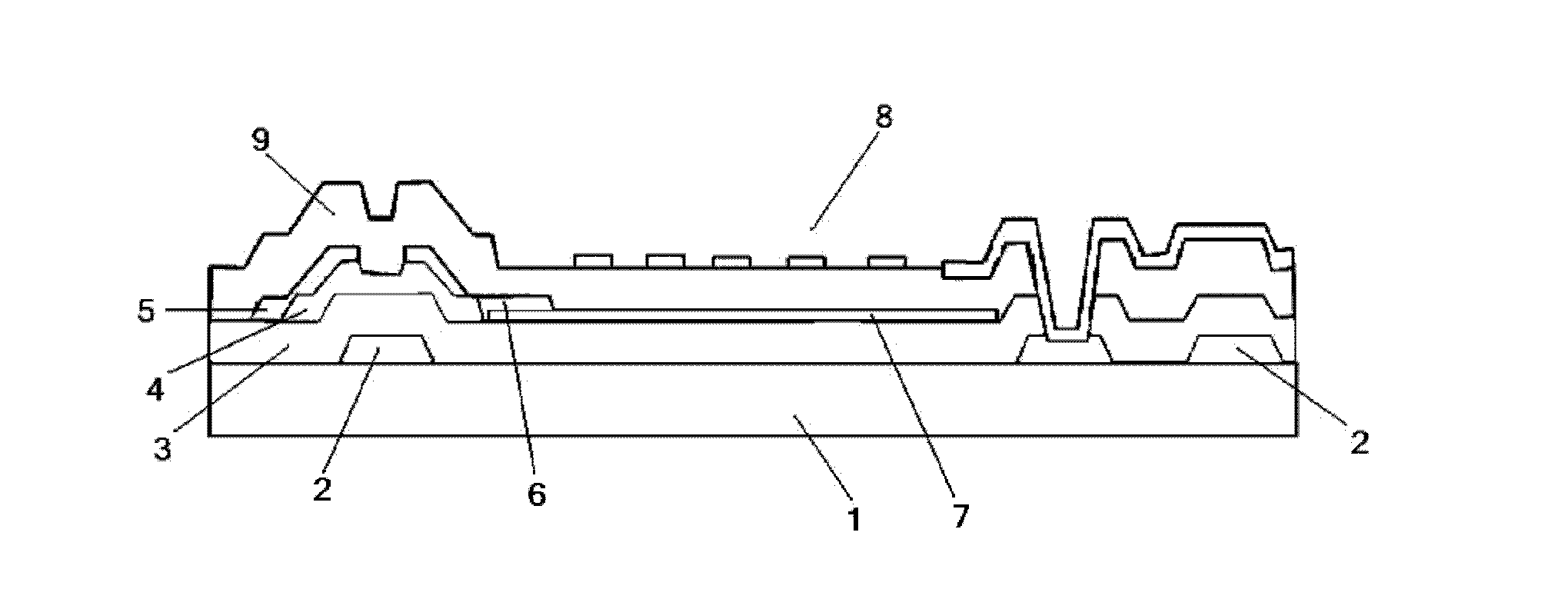
[0030] This embodiment specifically provides an array substrate, which can be applied in the ADS driving mode, such as figure 2 As shown, it includes a gate line and a data line that define a pixel area, the pixel area includes a thin film transistor area and a pixel electrode pattern area, and a gate 2, a gate insulating layer 3, an active layer are formed in the thin film transistor area 4. The source electrode 5, the drain electrode 6 and the passivation layer 9; the gate insulating layer 3, the pixel electrode 7, the passivation layer 9 and the common electrode 8 are formed in the pattern area of ​​the pixel electrode, wherein the common electrode The electrode 8 and the pixel electrode 7 constitute a multi-dimensional electric field; the protective layer 12 can be optionally covered above the gate insulating layer 3 and the source / drain and then a black matrix layer 10 is formed above the source / drain and the TFT channel, or The black matrix layer 10 is formed directly a...

Embodiment 2

[0053] This embodiment provides another array substrate. Since the above-mentioned Embodiment 1 has been described in detail, some repetitive content will be omitted in this embodiment, and only the differences will be described in detail here.

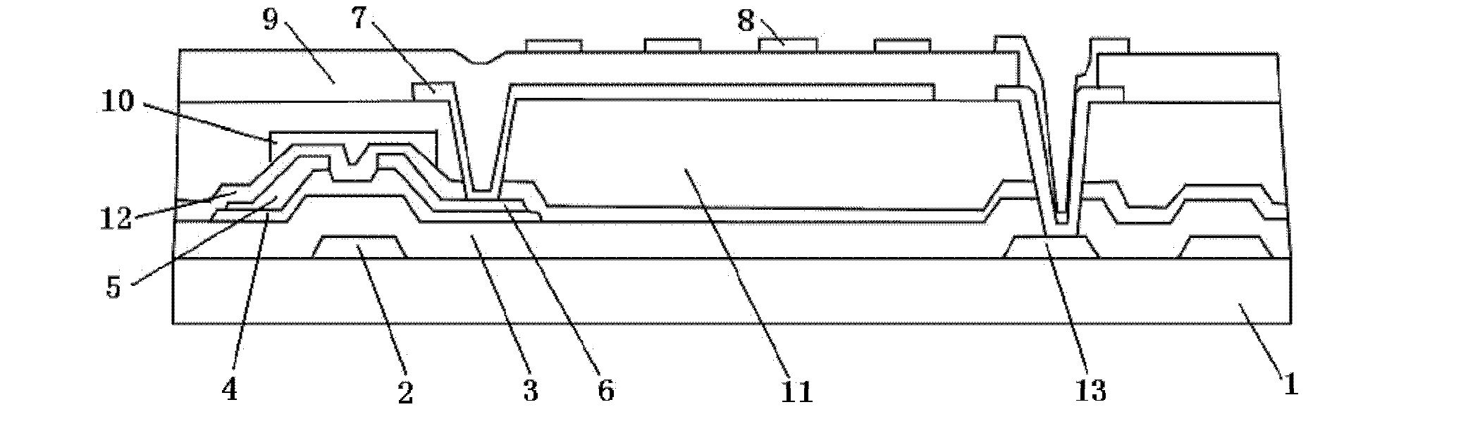
[0054] The array substrate provided by this embodiment can be applied in the ADS driving mode, such as Figure 4 As shown, it includes a gate line and a data line that define a pixel area, the pixel area includes a thin film transistor area and a pixel electrode pattern area, and a gate 2, a gate insulating layer 3, an active layer are formed in the thin film transistor area 4. The source electrode 5, the drain electrode 6 and the passivation layer 9; the gate insulating layer 3, the pixel electrode 7, the passivation layer 9 and the common electrode 8 are formed in the pattern area of ​​the pixel electrode, wherein the common electrode The electrode 8 and the pixel electrode 7 constitute a multi-dimensional electric field.

[0055] ...


PUM

PropertyMeasurementUnit
thicknessaaaaaaaaaa
thicknessaaaaaaaaaa
optical densityaaaaaaaaaa

Abstract

The invention relates to an array substrate, a method for manufacturing the array substrate and a display device comprising the array substrate, belonging to the technical field of displaying and aiming to solve the problem that the contrast of the existing liquid crystal panel is too low. The array substrate comprises a grid line and a data line for defining a pixel region; the pixel region comprises a thin film transistor region and a pixel electrode pattern region; a grid electrode, a grid insulating layer, an active layer, a source electrode, a drain electrode and a passivation layer are formed in the thin film transistor region; a grid insulating layer, a pixel electrode, a passivation layer and a common electrode are formed in the pixel electrode pattern region; a multidimensional electric field is formed by the common electrode and the pixel electrode; and a colored resin layer is formed between each grid insulating layer and each pixel electrode. According to the technical scheme provided by the invention, because a colored resin layer is formed above the grid insulating layer of a thin film transistor, the structure in the pixel region can be flattened, the irregular arrangement of the liquid crystal in the reflection region can be avoided, the light leakage can be prevented, and the contrast can be improved.

Description

technical field [0001] The present invention relates to the field of display technology, in particular to an array substrate, a manufacturing method thereof, and a display device including the array substrate. Background technique [0002] Thin Film Transistor Liquid Crystal Display (TFT-LCD for short) has the characteristics of small size, low power consumption, and no radiation, and occupies a dominant position in the flat panel display market. With the advancement of technology, consumers have put forward higher requirements for the display effect of mobile products, and the display effect of ordinary TN (Twisted Nematic, twisted nematic) liquid crystal display can no longer meet the market demand. At present, major manufacturers are gradually applying various wide viewing angle technologies with better display effects to mobile products, such as IPS (In-Plane Switching, coplanar switching), VA (Vertical Alignment, vertical alignment), AD-SDS (Advanced-Super Dimensional ...

Claims


Application Information

Patent Timeline
Patent Type & Authority Applications(China)
IPC IPC(8): G02F1/1362G02F1/1368G02F1/1343H01L27/12H01L21/77
CPCH01L27/1259G02F2001/134318G02F1/1362G02F2001/134372G02F1/1343G02F2001/136222H01L27/124G02F1/136209G02F2203/01G02F2203/02G02F1/134318G02F1/134372G02F1/136222G02F1/1368
Inventor 宋泳锡惠官宝刘圣烈崔承镇张锋
Owner BOE TECH GRP CO LTD
Why Eureka
Try Eureka