Projection objective lens wave aberration detection device and method

A technology of projection objective lens and detection device, which is applied to exposure device of photoengraving process, photography, testing optical performance, etc., can solve the problem of low accuracy of interferogram processing method, save measurement time, avoid system error, and achieve high phase shift accuracy Effect

Inactive Publication Date: 2012-09-19
INST OF OPTICS & ELECTRONICS - CHINESE ACAD OF SCI
View PDF7 Cites 53 Cited by
  • Summary
  • Abstract
  • Description
  • Claims
  • Application Information

AI Technical Summary

Problems solved by technology

[0007] The technical problem of the present invention is to overcome the deficiencies of the prior art and provide a projection objective lens wave aberration measurement device and method, which avoids the shortcomings of aberrations introduced by multiple gratings and collimating objective lenses and low precision of the interferogram processing method

Method used


Image

  • Projection objective lens wave aberration detection device and method
  • Projection objective lens wave aberration detection device and method
  • Projection objective lens wave aberration detection device and method

Examples


Embodiment Construction

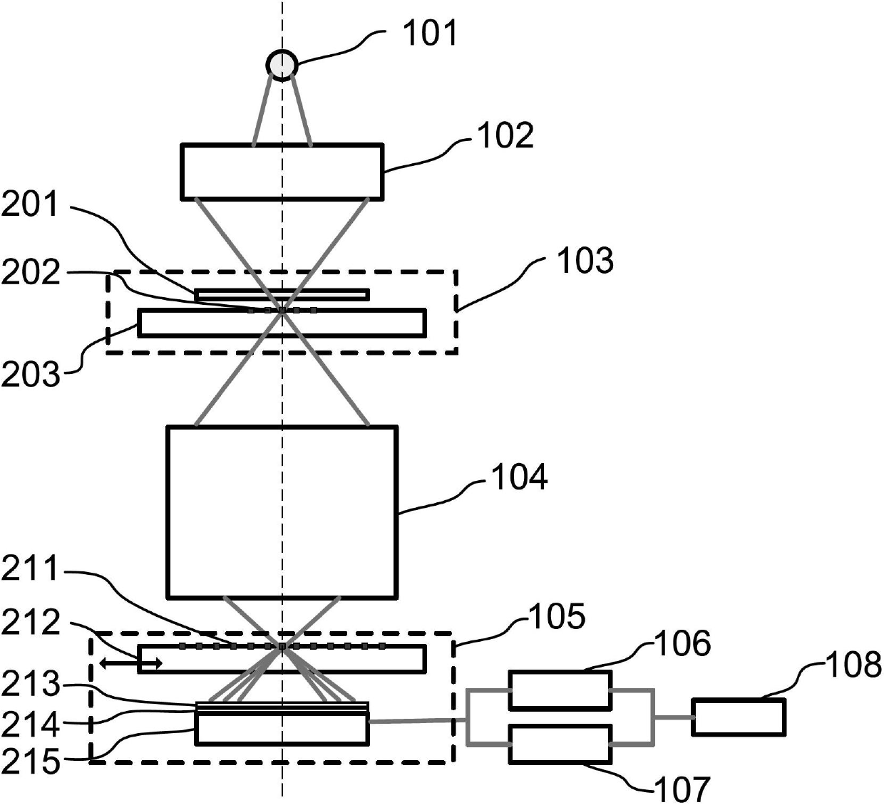
[0029] figure 1It is a schematic diagram of the projection objective lens wave aberration detection system of the present invention, which includes a light source 101, an illumination system 102, a secondary light source module 103, a measured projection objective lens 104, a detection module 105, an image collector 106, a controller 107, and a computer 108, Wherein: the secondary light source module 103 includes a scattering plate 201 , a mask plate 202 , and a mask stage 203 , and the detection module 105 includes a two-dimensional grating 211 , a silicon wafer stage 212 , a fluorescent material 213 , an optical filter 214 , and an area array detector 215 .

[0030] The light emitted by the light source 101 passes through the subsequent illumination system 102 to form a desired illumination mode and light field distribution on the mask surface of the lithography machine, providing light energy for subsequent detection and lithography. In the DUV exposure optical system, the ...


PUM


Abstract

The invention relates to a projection objective lens wave aberration detection device and method. Light emitted by a light source is uniformly radiated on a projection objective lens object plane, a scatter plate and a needle hole are installed on a masking stage, the needle hole is arranged on an object plane of a projection objective lens, the field of view is selected through the movement of the masking stage, a shearing grating is arranged on an image plane of the projection objective lens, the shearing grating is installed on a wafer stage together with a detector, the phase shifting function is realized through the transverse precise movement of the grating by the wafer stage, and simultaneously each frame of a shearing interference figure in the phase shifting process is recorded by utilizing the detector. Two-dimensional shearing is realized by utilizing the two-dimensional grating, the phase shifting function is integrated into the shearing interference instrument, and the high-precise measurement of the projection objective lens wave aberration is realized by adopting the characteristics of the phase space vector.

Description

technical field [0001] The invention relates to a wave aberration detection device and method of an optical system, in particular to a high-precision wave aberration detection device and method of a projection objective lens in a lithography projection exposure system. Background technique [0002] Optical projection lithography uses the principle of optical projection imaging to transfer the integrated circuit (IC) pattern on the mask to a rubber-coated silicon wafer by step-and-repeat or step-and-scan exposure. Optical projection lithography technology is currently the most effective method for large-scale and low-cost production of large-scale integrated circuits. This technology is also widely used in semiconductor industries such as flat panel display and semiconductor lighting, and plays a key role in the global informatization process. As the device density of very large-scale circuits (VLSI) is getting higher and higher, its feature size is getting smaller and smalle...

Claims


Application Information

Patent Timeline
Patent Type & Authority Applications(China)
IPC IPC(8): G03F7/20G01M11/02
CPCG03F7/706G03F7/7085
Inventor 刘志祥刘学峰吕保斌陈红丽甘大春何毅
Owner INST OF OPTICS & ELECTRONICS - CHINESE ACAD OF SCI
Why Eureka
Try Eureka