High-dynamic-range image sensor and manufacturing method thereof

An image sensor, high dynamic range technology, applied in radiation control devices and other directions, can solve the problems of anti-dark current increase, dark current noise increase, and inability to increase the size of the FD area.

Inactive Publication Date: 2012-09-19
北京三平桐益衡科技有限公司
View PDF3 Cites 8 Cited by
  • Summary
  • Abstract
  • Description
  • Claims
  • Application Information

AI Technical Summary

Problems solved by technology

[0007] In the prior art, in order to obtain a higher dynamic range, it is generally required to increase the size of the FD (floating diffusion) region to increase the capacitance of the FD region and increase the well capacity of the FD region, but this will also lead to an increase in dark current noise problems that affect image quality
In other words, it is necessary to increase the well capacity of the FD region to improve the dynamic range, but not to increase the size of the FD region to prevent the increase of dark current

Method used


Image

  • High-dynamic-range image sensor and manufacturing method thereof
  • High-dynamic-range image sensor and manufacturing method thereof
  • High-dynamic-range image sensor and manufacturing method thereof

Examples


Embodiment Construction

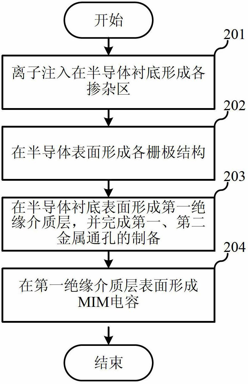
[0036] In the following description, many technical details are proposed in order to enable readers to better understand the application. However, those skilled in the art can understand that without these technical details and various changes and modifications based on the following implementation modes, the technical solution claimed in each claim of the present application can be realized.

[0037] In order to make the purpose, technical solution and advantages of the present invention clearer, the following will further describe the implementation of the present invention in detail in conjunction with the accompanying drawings.

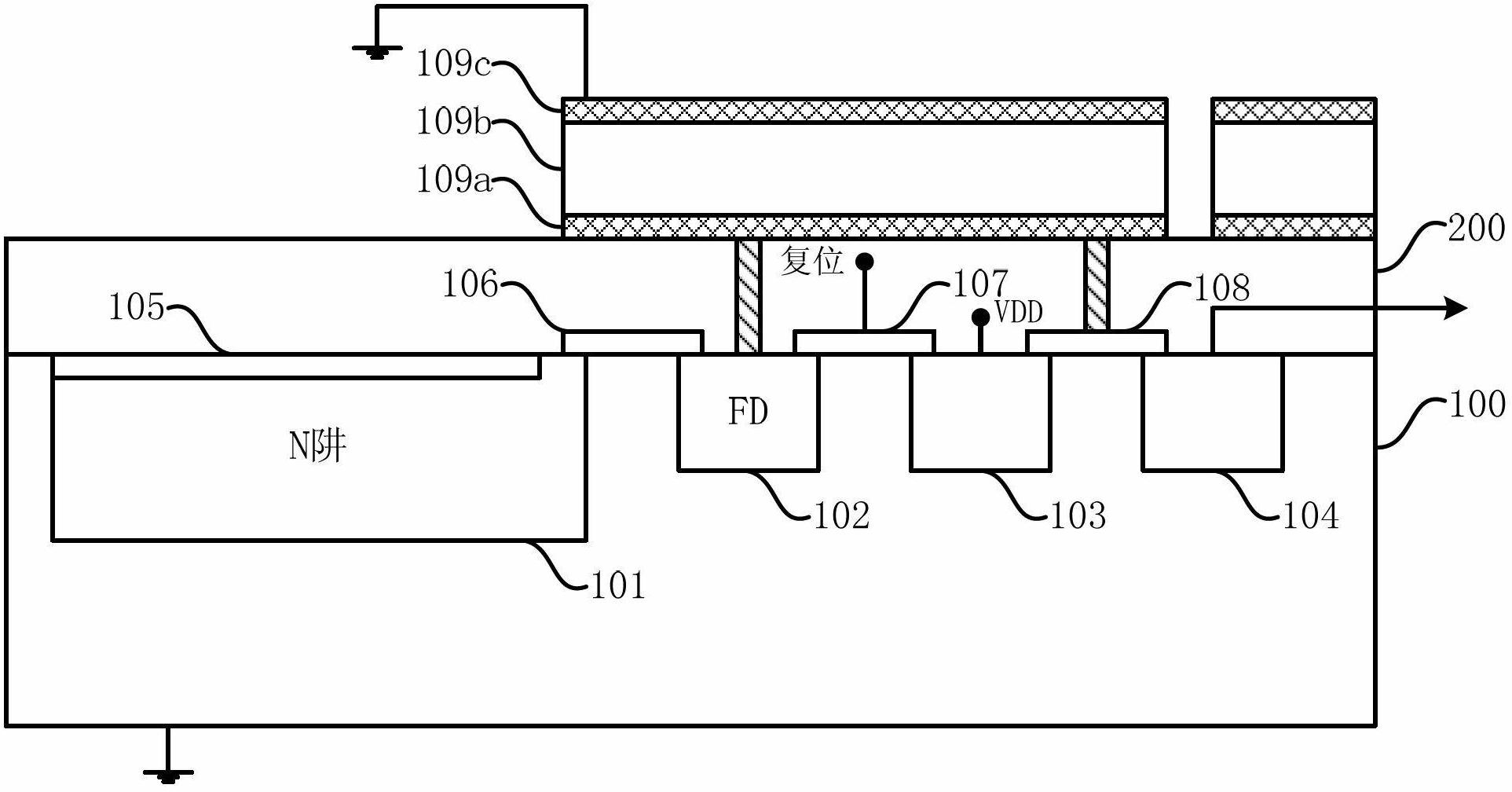
[0038] The first embodiment of the present invention relates to a high dynamic range image sensor. figure 1 It is a schematic diagram of the structure of the high dynamic range image sensor. The high dynamic range image sensor includes a metal wiring layer and an optical sensing layer separated by a first insulating medium layer 200 .

[0039] a...


PUM


Abstract

The invention relates to the field of semiconductor devices and discloses a high-dynamic-range image sensor and a manufacturing method thereof. According to the invention, a spare area in a metal wiring layer is ingeniously utilized, a metal-insulator-metal (MIM) capacitor is formed and connected in parallel with a floating diffusion area, the well capacity of the floating diffusion area is improved, and the storage capacity of photo-induced charges of the image sensor is improved, so the upper limit of a dynamic range is raised. Meanwhile, the self area of the floating diffusion area is not increased, so increase of dark current noise is avoided.

Description

technical field [0001] The invention relates to the field of semiconductor devices, in particular to the manufacturing technology of image sensors. Background technique [0002] The image sensor is one of the main components of a digital camera, and is widely used in digital imaging, aerospace and medical imaging and other fields. [0003] Image sensors can be divided into two categories: CCD (Charge Coupled Device, charge-coupled device) and CMOS (Complementary Metal-Oxide Semiconductor, metal oxide semiconductor element) according to different components. [0004] In addition to being widely used in digital cameras, CCD image sensors are also widely used in video cameras, scanners, and industrial fields. It is worth mentioning that CCD image sensors and related equipment are also widely used in the shooting of the inside of the human body for the purpose of diagnosing diseases or performing microsurgery in medicine. CCD image sensors are also widely used in astrophotogra...

Claims


Application Information

Patent Timeline
Patent Type & Authority Applications(China)
IPC IPC(8): H01L27/146
Inventor 苗田乐方娜田犁汪辉陈杰
Owner 北京三平桐益衡科技有限公司
Why Eureka
Try Eureka