Flat-grid electric charge storage type IGBT (insulated gate bipolar translator)

A charge storage and charge storage layer technology, applied in circuits, electrical components, semiconductor devices, etc., can solve the problems of small device breakdown voltage and reduced device breakdown voltage, and achieve the effect of good breakdown voltage and optimized compromise

Inactive Publication Date: 2012-09-19
UNIV OF ELECTRONICS SCI & TECH OF CHINA +1
View PDF3 Cites 21 Cited by
  • Summary
  • Abstract
  • Description
  • Claims
  • Application Information

AI Technical Summary

Problems solved by technology

However, for the planar gate charge storage type IGBT, due to the existence of the N-type charge storage layer with a higher doping concentration, the breakdown voltage of the device is significantly reduced, and the higher the doping concentration of the N-type charge storage layer, the breakdown voltage of the device The smaller the voltage

Method used


Image

  • Flat-grid electric charge storage type IGBT (insulated gate bipolar translator)
  • Flat-grid electric charge storage type IGBT (insulated gate bipolar translator)
  • Flat-grid electric charge storage type IGBT (insulated gate bipolar translator)

Examples


Embodiment Construction

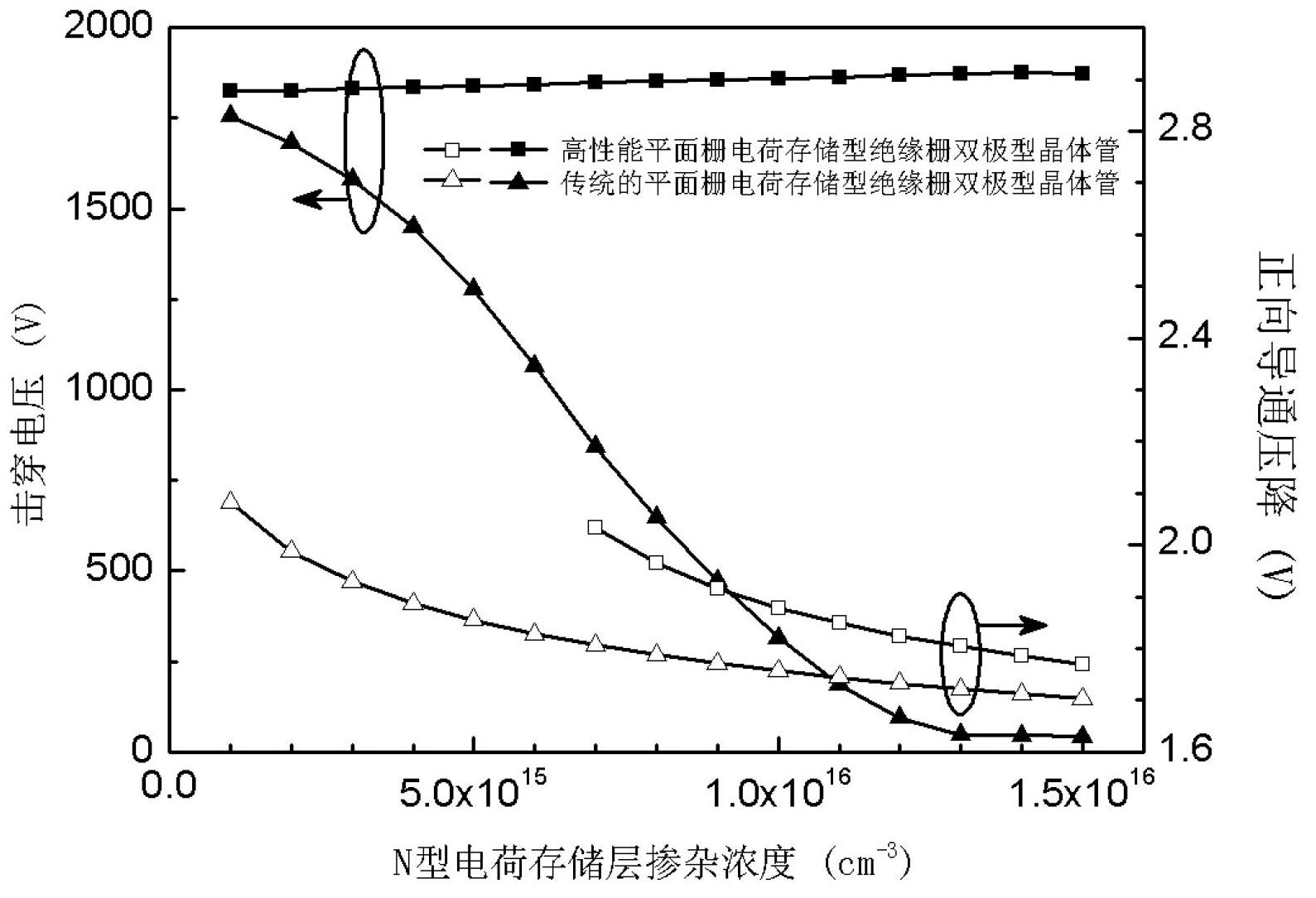
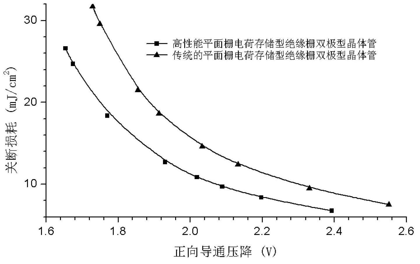
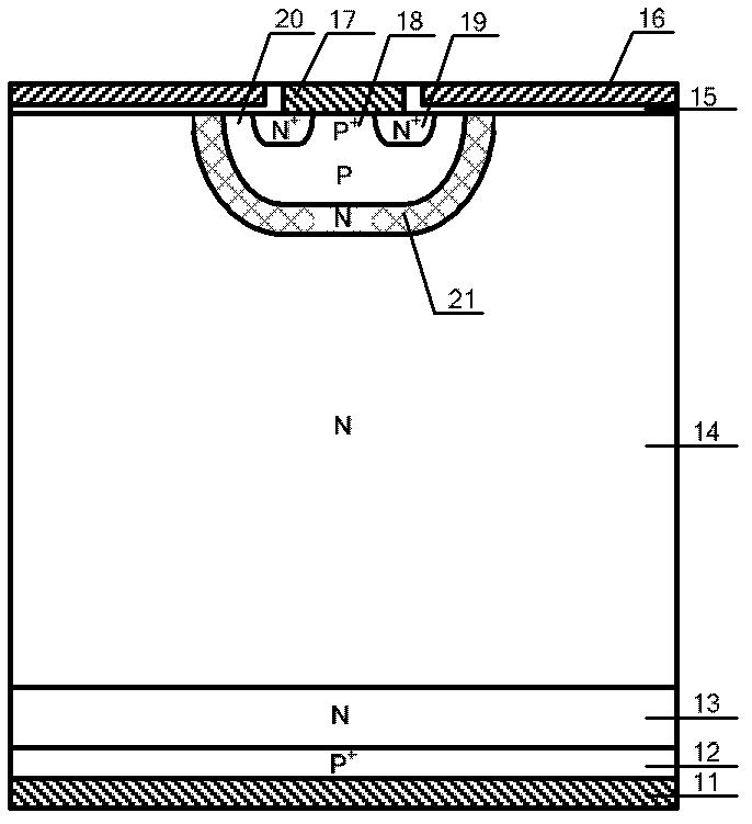
[0019] A planar gate charge storage type IGBT, such as Figure 2 to Figure 3 shown, including P + collector 12, located at P + The metal collector 11 on the back of the collector 12 is located at P + The N on the front of the collector 12 + Electric field blocking layer 13, located at N + N on the surface of the electric field stop layer 13 - Drift zone 14, located at N - The P-type base region 20 in the middle of the top of the drift region 14, and the two Ns located inside the P-type base region 20 + The contact region 19 is located inside the P-type base region 20 and is located between the two N + P between the contact area 19 + Contact region 18, located on the device surface and connected to two N + Contact zone 19 and P + The metal emitter 17 contacted by the contact region 18 is located on the surface of the device and is connected to the two N + Contact region 19, P-type base region 20 and N - The gate oxide layer 15 in contact with the drift region 14, the...


PUM


Abstract

The invention provides a flat-grid electric charge storage type IGBT (insulated gate bipolar translator), belonging to the technical field of a power semiconductor device. On the basis of the conventional flat-grid electric charge storage type IGBT, a layer of P type buried layer is induced between an N type drift region and an N type electric charge storage layer; due to the electric field modulating action of an additive PN (positive/negative) junction and the electric charge induced into the P type buried layer, the adverse impact of a highly-doped N type electric charge storage layer to the device is screened, so that the device can obtain high puncture voltage; and due to the electric field screening action of the P type buried layer to the N type electric charge storage layer, the IGBT can adopt higher N type electric charge storage layer doping concentration, so that the conductivity modulation of the N type drift region of the device can be enhanced, and the carrier distribution in the N type drift region can be optimized, and therefore, the device is lower in forward conductivity voltage drop and relatively good in compromises between the forward conductivity voltage drop and the turn-off loss. The IGBT is applicable to the filed of the semiconductor device and a power integrated circuit from small power to high power.

Description

technical field [0001] The invention belongs to the technical field of power semiconductor devices, and relates to an insulated gate bipolar transistor (IGBT), more specifically, to a planar gate charge storage type insulated gate bipolar transistor. Background technique [0002] Insulated Gate Bipolar Transistor (IGBT) is a new type of power electronic device combining MOS field effect and bipolar transistor. It not only has the advantages of easy driving and simple control of MOSFET, but also has the advantages of low conduction voltage of power transistor, large on-state current and small loss. It has become one of the core electronic components in modern power electronic circuits and is widely used in Various fields of the national economy such as communications, energy, transportation, industry, medicine, household appliances and aerospace. The application of IGBT plays an extremely important role in improving the performance of power electronic systems. Since the inv...

Claims


Application Information

Patent Timeline
Patent Type & Authority Applications(China)
IPC IPC(8): H01L29/739
CPCH01L29/7395
Inventor 张金平夏小军王娜李长安张蒙李泽宏任敏张波
Owner UNIV OF ELECTRONICS SCI & TECH OF CHINA
Why Eureka
Try Eureka