Check patentability & draft patents in minutes with Patsnap Eureka AI!

Dry etching method for grooves

A technology of dry etching and trenching, which is applied to electrical components, semiconductor/solid-state device manufacturing, circuits, etc., can solve the problem that metal fillers cannot fill through-silicon holes, etc., and achieve the effect of reducing size and increasing windows

Inactive Publication Date: 2012-09-26
SHANGHAI HUAHONG GRACE SEMICON MFG CORP
View PDF7 Cites 1 Cited by
  • Summary
  • Abstract
  • Description
  • Claims
  • Application Information

AI Technical Summary

Problems solved by technology

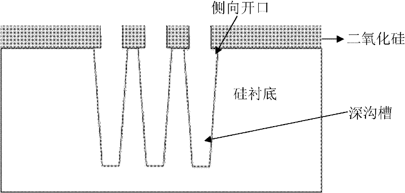
The deep hole or deep trench is obtained by a dry etching process, and since the aspect ratio is too large, there will be a problem of lateral opening (undercut) after dry etching (see figure 1 ), the lateral opening exists between the pre-metal dielectric layer (PMD) and the TSV, and the lateral opening will cause the subsequent metal filling to fail to fill the TSV

Method used


Image

  • Dry etching method for grooves
  • Dry etching method for grooves
  • Dry etching method for grooves

Examples


Embodiment Construction

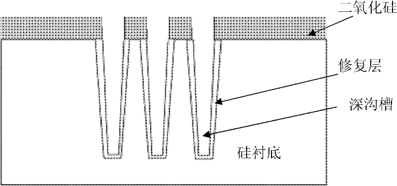
[0011] The dry etching method of the groove of the present invention is to form a repair layer on the side wall of the groove by using a selective silicon epitaxial growth process after etching the groove in the silicon substrate to compensate for the defects formed in the etching. Side opening.

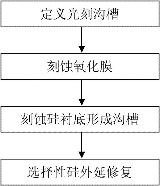
[0012] In a specific embodiment, the trench etching process includes the following steps (see image 3 ).

[0013] The position and size of the grooves are first defined on the silicon substrate by photolithography. Prior to this, a silicon oxide layer is usually deposited on a silicon substrate. The photolithography process includes coating a photoresist on a silicon substrate, exposing it with a photolithography mask, and developing it to form a photoresist pattern. In a specific implementation, the thickness of the photoresist should be as thick as possible to withstand the subsequent dry etching. The photoresist thickness is generally above 3 microns.

[0014] Then use photo...


PUM


Abstract

The invention discloses a dry etching method of grooves, which repairs openings of the side walls of the grooves by applying a selective epitaxy technology after grooves are formed by the dry etching method. The method of the present invention repairs the side openings due to etching by applying the selective epitaxy technology after the etching of grooves.

Description

technical field [0001] The invention relates to a dry etching process of grooves. Background technique [0002] The through silicon via (TSV) process is an emerging integrated circuit manufacturing process, which is suitable for various performance improvements. It is used in power amplifiers in wireless local area networks and mobile phones, and will greatly improve the frequency characteristics and power characteristics of the circuit. The through-silicon via technology connects the circuit fabricated on the upper surface of the silicon chip to the back of the silicon chip through the metal filled in the through-silicon hole. Combined with the three-dimensional packaging process, the IC layout develops from the traditional two-dimensional side-by-side arrangement to a more advanced three-dimensional stacking, so that components The package is more compact, and the chip lead distance is shorter, which can greatly improve the frequency characteristics and power characteristi...

Claims


Application Information

Patent Timeline
IPC IPC(8): H01L21/311H01L21/20
Inventor 吴智勇刘继全杨华
Owner SHANGHAI HUAHONG GRACE SEMICON MFG CORP
Features
  • R&D
  • Intellectual Property
  • Life Sciences
  • Materials
  • Tech Scout
  • Unparalleled Data Quality
  • Higher Quality Content
  • 60% Fewer Hallucinations
Learn More