Semiconductor device and manufacturing method thereof
What is Al technical title?
Al technical title is built by PatSnap Al team. It summarizes the technical point description of the patent document.
A manufacturing method and semiconductor technology, applied in the direction of semiconductor devices, final product manufacturing, sustainable manufacturing/processing, etc., can solve the problems of weak response signal strength and high unit production cost, and achieve the effect of facilitating absorption and simple manufacturing process
Active Publication Date: 2012-09-26
INST OF MICROELECTRONICS CHINESE ACAD OF SCI
View PDF5 Cites 21 Cited by
Summary
Abstract
Description
Claims
Application Information
AI Technical Summary
This helps you quickly interpret patents by identifying the three key elements:
Problems solved by technology
Method used
Benefits of technology
Problems solved by technology
[0006] The technical problem to be solved in the present invention is to overcome the problems of weak response signal strength and high unit production cost of traditional ultraviolet detectors, and provide a new type of high-efficiency, simple, low-cost and large-area device structure for ultraviolet detection
Method used
Image
Click on the blue label to locate the original text in one second.
Reading with bidirectional positioning of images and text.
Examples
Embodiment Construction
[0021] In order to make the objectives, technical solutions and advantages of the present invention clearer, the features and technical effects of the technical solutions of the present invention will be described in detail below with reference to the accompanying drawings and in conjunction with illustrative embodiments. A low-cost large-size amorphous material is disclosed. State oxide semiconductor TFT type ultraviolet detector and its manufacturing method. It should be pointed out that similar reference signs indicate similar structures, and the terms "first", "second", "upper", "lower", etc. used in this application can be used to modify various device structures. Unless otherwise specified, these modifications do not imply the spatial, order, or hierarchical relationship of the modified device structure.
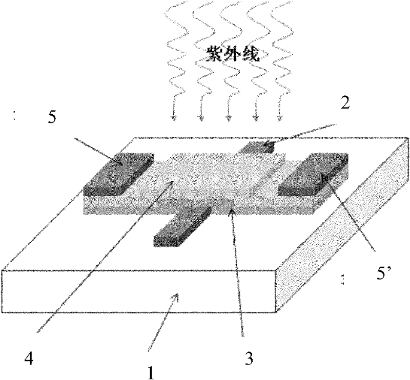
[0022] Such as figure 1 As shown, the present invention is a thin film transistor (TFT) type ultraviolet detection device, which includes a substrate 1, a back gate elect...
PUM
Abstract
The invention provides a semiconductor device, comprising a substrate, a gate electrode on the substrate, a gate insulating layer on the gate electrode, an amorphous oxide semiconductor on the gate insulating layer and source and drain metal electrodes on the amorphous oxide semiconductor at two sides of the gate electrode, and the basic structure is a TFT ultraviolet detector. The semiconductor is an amorphous oxide semiconductor with a broad bang [band] gap (>3.0eV), and the material component can be a ZnO semiconductor doped with In, specifically comprising InGaZnO, InZanO, HfInZnO, TaInZnO, ZrInZnO, YInZnO, AlInZnO and SnInZnO; wherein the atomic counting ratio of [In] to a sum of [In] and [a third metal] is from 35% to 80%, and the atomic counting ratio of [Zn] to a sum of [In] and [Zn] is from 40% to 85%. Preferable atomic counting ratio of elements is that the ratio of [In], [the third metal], [Zn], and [O] is 1:1:1:1 or 1:1:1:2 or 2:2:2:1, or 1:1:1:4, etc. In addition, the semiconductor can be of a material such as In2O3, ZTO, ITO, ZnO, SnOx in an amorphous state. The TFT ultraviolet detector based on the invention has advantages of high efficiency, low cost and evenness for a large area due to the adoption of the amorphous oxide semiconductor.
Description
Technical field [0001] The invention relates to a semiconductor device and a manufacturing method thereof, in particular to a thin film transistor (TFT) type ultraviolet detector of a low-cost large-size amorphous oxide semiconductor and a manufacturing method thereof. Background technique [0002] In recent years, with the continuous deepening of research and exploration in the fields of astronomy, high-energy physics, and space technology, higher requirements have been put forward for ultraviolet detection technology and detection materials. Ultraviolet (UV) detection technology is another dual-use photoelectric detection technology developed after infrared and laser detection technology. It has high application value in both military and civil applications. In the military, ultraviolet detection technology can be used in missile guidance, missile early warning, ultraviolet communications, ultraviolet interference, optoelectronic countermeasures and other fields, which have att...
Claims
Application Information
Patent Timeline
Application Date:The date an application was filed.
Publication Date:The date a patent or application was officially published.
First Publication Date:The earliest publication date of a patent with the same application number.
Issue Date:Publication date of the patent grant document.
PCT Entry Date:The Entry date of PCT National Phase.
Estimated Expiry Date:The statutory expiry date of a patent right according to the Patent Law, and it is the longest term of protection that the patent right can achieve without the termination of the patent right due to other reasons(Term extension factor has been taken into account ).
Invalid Date:Actual expiry date is based on effective date or publication date of legal transaction data of invalid patent.
Patent Type & Authority Applications(China)
IPC IPC(8): H01L31/112H01L31/18
CPCY02P70/521Y02P70/50
Inventor 殷华湘陈大鹏
Owner INST OF MICROELECTRONICS CHINESE ACAD OF SCI