Patterned substrate, mask and patterned substrate manufacturing method

A technology of a patterned substrate and a manufacturing method, applied in the field of LED technology, can solve the problems of no purpose, random light propagation direction, etc., and achieve the effects of simple structure, improved axial luminous brightness, and simple preparation

Active Publication Date: 2012-09-26
HANGZHOU SILAN AZURE
View PDF4 Cites 7 Cited by
  • Summary
  • Abstract
  • Description
  • Claims
  • Application Information

AI Technical Summary

Problems solved by technology

But this kind of structure is designed based on the principle of diffuse reflection of light afte...

Method used


Image

  • Patterned substrate, mask and patterned substrate manufacturing method
  • Patterned substrate, mask and patterned substrate manufacturing method
  • Patterned substrate, mask and patterned substrate manufacturing method

Examples


Embodiment Construction

[0052] In order to make the content of the present invention clearer and easier to understand, the content of the present invention will be further described below in conjunction with the accompanying drawings. Of course, the present invention is not limited to this specific embodiment, and general replacements known to those skilled in the art are also covered within the protection scope of the present invention.

[0053] Secondly, the present invention is described in detail by means of schematic diagrams. When describing the examples of the present invention in detail, for the convenience of explanation, the schematic diagrams are not partially enlarged according to the general scale, which should not be used as a limitation of the present invention.
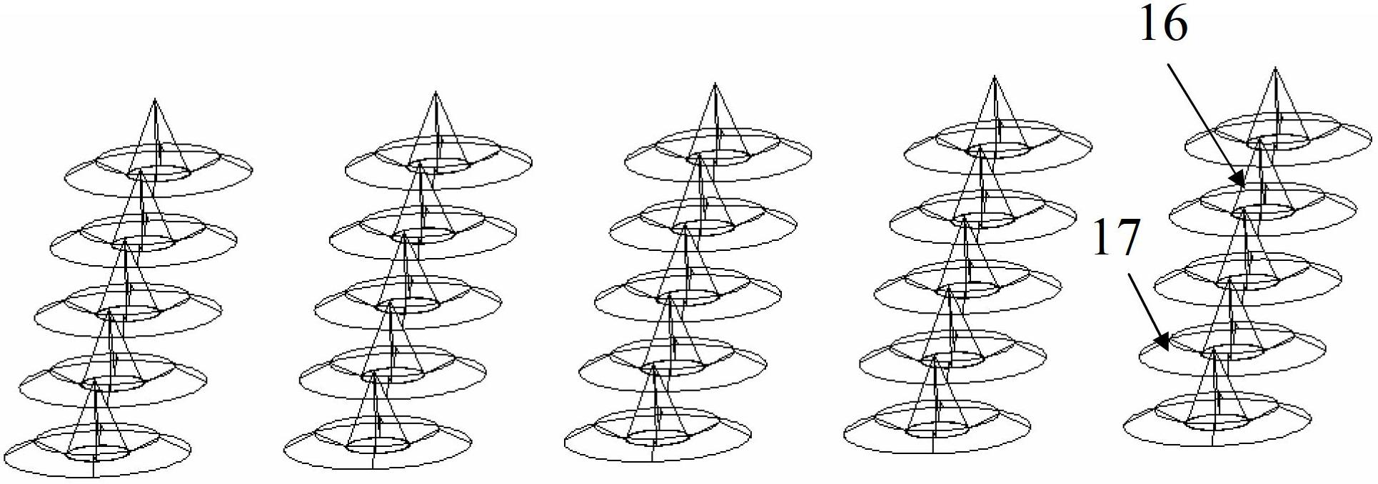
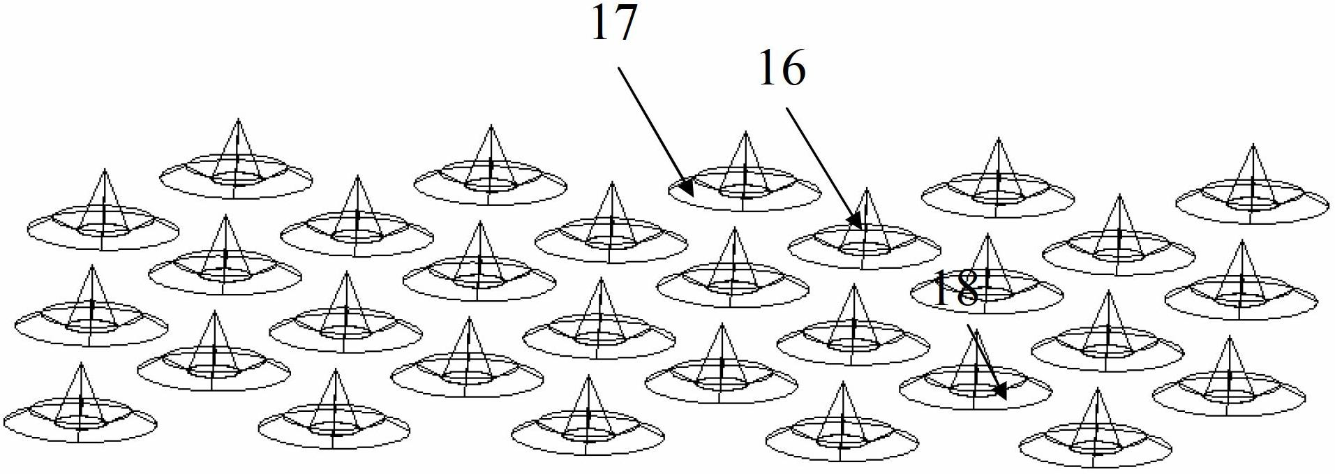
[0054] The core idea of ​​the present invention is: the present invention provides a patterned substrate with a microstructure composed of a luminous body and a reflective bowl, thereby greatly improving the axial luminance of...


PUM

PropertyMeasurementUnit
Bottom diameteraaaaaaaaaa
Heightaaaaaaaaaa
Heightaaaaaaaaaa

Abstract

The invention provides a patterned substrate, a mask used for manufacturing the patterned substrate and a patterned substrate manufacturing method. The patterned substrate is a patterned substrate with microstructures which consist of kinds of luminous bodies and reflecting bowls, can greatly improve the luminance of an LED (light-emitting diode) chip and can especially improve axial luminance. Masks which form the patterned substrate use pinhole diffraction and filter principles, the structure is simple, the special design is not required, the masks are easy to prepare and the cost is low. The patterned substrate manufacturing method adopts a pinhole diffraction exposure and ICP (inductively coupled plasma) etching method, the process is simple, the method is easy to realize, the progress of introducing concepts and structure of macroscopic fields into the microscopic LED field to improve the axial luminance of the LED chip is accelerated.

Description

technical field [0001] The invention relates to the field of LED technology, in particular to a patterned substrate capable of improving the axial luminance of an LED chip, a mask for making the patterned substrate, and a method for manufacturing the patterned substrate. Background technique [0002] The original LED process is to grow N-GaN, quantum well, P-GaN and other stacked epitaxial structures on a flat substrate, then form a transparent conductive film on the stacked epitaxial structure and open holes, and finally make P and N electrodes and A passivation protection layer structure is formed. When LEDs have developed to the stage of landscape lighting and general lighting, the luminous brightness of LEDs has encountered higher challenges. In the case of limited space for improving the internal quantum efficiency (already close to 100%), in order to further improve the performance of LEDs To improve the luminous brightness, researchers in the LED industry have introd...

Claims


Application Information

Patent Timeline
IPC IPC(8): H01L33/10H01L33/00G03F1/00G03F7/00
Inventor 丁海生李东昇马新刚江忠永张昊翔王洋李超黄捷黄敬
Owner HANGZHOU SILAN AZURE
Why Eureka
Try Eureka