Platinum-silicon nanowire infrared detector and manufacturing method thereof

An infrared detector and silicon nanowire technology, applied in the field of infrared detectors, can solve the problems of low quantum efficiency of platinum-silicon infrared detectors, achieve the effects of reducing noise and dark current, simplifying the packaging process, and improving quantum efficiency

Active Publication Date: 2014-05-14
CETC CHIPS TECH GRP CO LTD
View PDF4 Cites 7 Cited by
  • Summary
  • Abstract
  • Description
  • Claims
  • Application Information

AI Technical Summary

Problems solved by technology

[0002] The platinum silicon infrared focal plane array device made of PtSi / P-Si Schottky barrier detector has the characteristics of high pixel integration, good photoresponse uniformity, good chip stability, etc., and has a wide range of applications. Compared with HgTeCd infrared detectors, the quantum efficiency of platinum-silicon infrared detectors is more than an order of magnitude lower; for many years, technicians have been committed to improving the quantum efficiency of platinum-silicon infrared detectors.

Method used


Image

  • Platinum-silicon nanowire infrared detector and manufacturing method thereof

Examples


Embodiment Construction

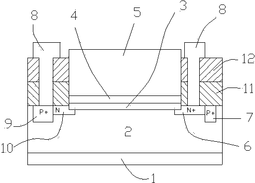
[0027] A platinum-silicon nanowire infrared detector, the structure of which is: the platinum-silicon nanowire infrared detector comprises a P-type epitaxial silicon substrate layer 2, a platinum-silicon thin film photosensitive layer 3, a P-type polysilicon capping layer 4, and an anti-reflection film layer 5. P-type epitaxial silicon substrate layer 2, platinum silicon thin-film photosensitive layer 3, P-type polysilicon capping layer 4, and anti-reflection film layer 5 are stacked together in sequence; the platinum-silicon thin-film photosensitive layer 3 is platinum silicon nanowire; The working mode of the platinum-silicon nanowire infrared detector described above adopts the positive illumination method.

[0028] Further, the platinum-silicon nanowire infrared detector is also provided with an output diode 6 , a P+ channel resistance 7 , an electrode lead 8 , a P+ diffusion ground 9 and an N guard ring 10 .

[0029] Further, an aluminum mirror layer 1 is stacked on the b...


PUM


Abstract

A platinum-silicon nanowire infrared detector comprises a P-type epitaxial silicon substrate layer, a platinum-silicon film photo-sensitive layer, a P-type polycrystalline silicon cap layer and an antireflection film layer. The P-type epitaxial silicon substrate layer, the platinum-silicon film photo-sensitive layer, the P-type polycrystalline silicon cap layer and the antireflection film layer are sequentially overlapped. The platinum-silicon film photo-sensitive layer is a platinum-silicon nanowire, and the platinum-silicon nanowire infrared detector works in a front illumination mode. The platinum-silicon nanowire infrared detector has the advantages that absorptive rate can be increased through the platinum-silicon nanowire, a huge fringing field exists at the top end of the platinum-silicon nanowire to generate an avalanche multiplication effect, and the quantum efficiency of the platinum-silicon nanowire infrared detector is substantially improved; through the P-type polycrystalline silicon cap layer, the escape probability of photoproduction hot holes can be doubled, exchange of movable electric charges and photoproduction free electrons in the antireflection film layer is prevented, noise and dark currents of the platinum-silicon nanowire infrared detector are reduced, the front illumination mode is adopted in the detector, the packaging technology is substantially simplified, and reliability of the detector is improved.

Description

technical field [0001] The invention relates to an infrared detector, in particular to a platinum-silicon nanowire infrared detector and a manufacturing method thereof. Background technique [0002] The platinum silicon infrared focal plane array device made of PtSi / P-Si Schottky barrier detector has the characteristics of high pixel integration, good photoresponse uniformity, good chip stability, etc., and has a wide range of applications. , HgTeCd infrared detectors, platinum-silicon infrared detector quantum efficiency of more than one order of magnitude lower; for many years, technicians have been committed to improving the quantum efficiency of platinum-silicon infrared detector research. Contents of the invention [0003] Aiming at the problems in the background technology, the present invention proposes a platinum-silicon nanowire infrared detector, the structure of which is: the platinum-silicon nanowire infrared detector includes a P-type epitaxial silicon sub...

Claims


Application Information

Patent Timeline
Patent Type & Authority Applications(China)
IPC IPC(8): H01L31/101H01L31/0352H01L31/18
CPCH01L31/035227H01L31/1804Y02P70/50
Inventor 李华高熊平钟四成
Owner CETC CHIPS TECH GRP CO LTD
Why Eureka
Try Eureka