Nanometer/micrometer composite graphical sapphire substrate and preparation method thereof

A sapphire substrate and composite patterning technology, which is applied in chemical instruments and methods, separation methods, semiconductor/solid-state device manufacturing, etc., can solve the problems of low light extraction efficiency of GaN-based LEDs, and increase internal quantum efficiency and light extraction efficiency , Improve crystal quality, change the effect of propagation direction

Inactive Publication Date: 2017-02-08
SOUTH CHINA UNIV OF TECH
View PDF6 Cites 7 Cited by
  • Summary
  • Abstract
  • Description
  • Claims
  • Application Information

AI Technical Summary

Problems solved by technology

[0008] The present invention aims at the shortcomings of the existing micron-scale patterned sapphire substrate, that is, the problem that the light extraction efficiency of GaN-based LEDs prepared on the micron-scale patterned sapphire substrate is low, and proposes a more A sapphire substrate with nano-micron composite patterns that effectively improves the light extraction efficiency of GaN-based LEDs and improves the crystal quality of GaN thin films, and at the same time provides a preparation method for the sapphire substrate with nano-micron composite patterns

Method used


Image

  • Nanometer/micrometer composite graphical sapphire substrate and preparation method thereof
  • Nanometer/micrometer composite graphical sapphire substrate and preparation method thereof
  • Nanometer/micrometer composite graphical sapphire substrate and preparation method thereof

Examples


Embodiment 1

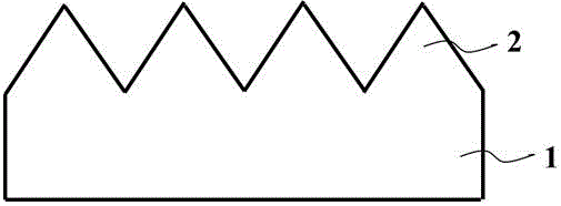
[0035] (1) Preparing micron-scale patterns 2 on the sapphire substrate 1;

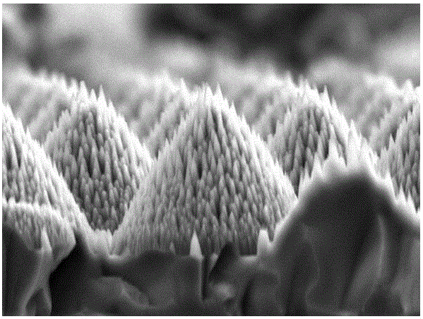
[0036] The existing conventional photolithography and ICP dry etching processes are adopted. First spin coat a layer of photoresist on the flat sapphire substrate, the thickness of the photoresist is 3 μm; use a photolithography machine to expose and develop to obtain a mask pattern; use the photoresist as a mask. The sapphire substrate is etched with an ICP device to obtain a sapphire substrate 1 with micron-scale patterns 2 . Micron-scale figure 2 is a cone with a height of 1 μm and a base radius of 2 μm.

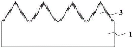
[0037] (2) Cleaning the substrate, and then using a magnetron sputtering system to deposit a nickel film with a thickness of 10nm on the micron-scale pattern 2;

[0038] (3) Put the substrate on which the nickel film was deposited in step (2) into a rapid annealing furnace, and anneal in a nitrogen atmosphere at an annealing temperature of 850°C for 180 seconds, so that the nickel film is agglomer...

Embodiment 2

[0047] (1) Preparing micron-scale patterns 2 on the sapphire substrate 1;

[0048] The existing conventional photolithography and ICP dry etching processes are adopted. First spin coat a layer of photoresist on the flat sapphire substrate, the thickness of the photoresist is 3 μm; use a photolithography machine to expose and develop to obtain a mask pattern; use the photoresist as a mask. The sapphire substrate is etched with an ICP device to obtain a sapphire substrate 1 with micron-scale patterns 2 . The micron-scale pattern 2 is a truncated cone with a height of 3 μm and a base radius of 6 μm.

[0049] (2) Cleaning the substrate, and then using a magnetron sputtering system to deposit a nickel film with a thickness of 20nm on the micron-scale pattern 2;

[0050] (3) Put the substrate on which the nickel film was deposited in step (2) into a rapid annealing furnace, and anneal in a nitrogen atmosphere at an annealing temperature of 850°C for 180 seconds, so that the nickel...


PUM

PropertyMeasurementUnit
heightaaaaaaaaaa
diameteraaaaaaaaaa
heightaaaaaaaaaa

Abstract

The invention provides a nanometer/micrometer composite graphical sapphire substrate and a preparation method thereof. The sapphire substrate has a composite pattern which is obtained through compositing a nanometer-scale pattern and a micrometer-scale pattern. The preparation method comprises the steps of preparing the micrometer-scale pattern on the sapphire substrate; depositing a nickel film on the micrometer-scale pattern; aggregating the nickel film for obtaining a large number of nickel nanometer particles; transferring the pattern of the nickel nanometer particles to the sapphire substrate according to dry-method etching through using the nickel nanometer particles as a mask, and forming a nanometer pattern on the micrometer-scale pattern of the sapphire substrate; eliminating nickel nanometer particle corrosion; and cleaning the substrate for finally obtaining the sapphire substrate with the nanometer/micrometer composite pattern. The nanometer/micrometer composite graphical sapphire substrate and the preparation method thereof have advantages of performing nanometer coarsening on the micrometer-scale pattern, improving epitaxial lateral growth, further improving crystal quality of the epitaxial film, more effectively changing light propagation direction, increasing light outlet probability, and improving internal quantum efficiency and light extraction efficiency of GaN-base LED of the sapphire substrate.

Description

technical field [0001] The invention relates to the technical field of semiconductor crystal preparation, in particular to a nano / micro composite patterned sapphire substrate and a preparation method thereof. Background technique [0002] GaN is a wide bandgap semiconductor material, and it can form a ternary or quaternary solid solution with other group III nitrides (InN, AlN). Both optoelectronics and microelectronics have great application potential, therefore, GaN is called "the third generation semiconductor material". At present, GaN-based LEDs, as a new generation of light sources, are gradually replacing traditional light sources and are widely used in different fields such as display backlight, communication, outdoor display, and general lighting. [0003] GaN-based LEDs are already commercial products, but due to the continuous improvement of the market's performance requirements, there is a lot of power and space to further improve the photoelectric conversion ...

Claims


Application Information

Patent Timeline
Patent Type & Authority Applications(China)
IPC IPC(8): H01L33/20H01L33/00H01L21/3065B81B1/00B81C1/00
CPCH01L33/20B81B1/00B81C1/00206H01L21/3065H01L33/0066
Inventor 周泉斌徐明升王洪
Owner SOUTH CHINA UNIV OF TECH
Why Eureka
Try Eureka