Middle concentration P-type doping transmission type gallium arsenide optical cathode material and method for preparing same

A technology of gallium arsenide light and cathode material, which is applied in the fields of photo-emission cathode, main electrode of discharge tube, semiconductor/solid-state device manufacturing, etc. The effect of less dislocation, improved photoelectric sensitivity, and low doping concentration

Inactive Publication Date: 2005-06-29
INST OF SEMICONDUCTORS - CHINESE ACAD OF SCI
View PDF0 Cites 6 Cited by
  • Summary
  • Abstract
  • Description
  • Claims
  • Application Information

AI Technical Summary

Problems solved by technology

The activation efficiency of silver-cesium-oxygen (Ag-Cs-O) photocathode is low, and the photoelectric sensitivity of the photocathode is low

Method used


Image

  • Middle concentration P-type doping transmission type gallium arsenide optical cathode material and method for preparing same
  • Middle concentration P-type doping transmission type gallium arsenide optical cathode material and method for preparing same
  • Middle concentration P-type doping transmission type gallium arsenide optical cathode material and method for preparing same

Examples


Embodiment Construction

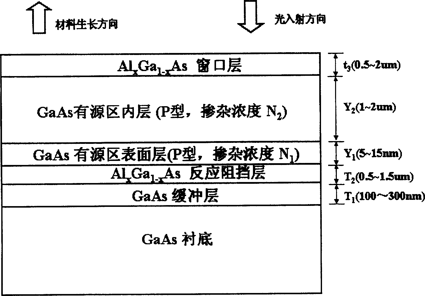
[0025] Combined with Figure 1 below, figure 2 , image 3 Describe in detail the structural details and working conditions of the concentration P-type doped transmissive gallium arsenide (GaAs) photocathode material in the specific implementation of the present invention.

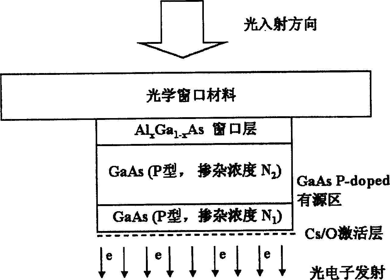
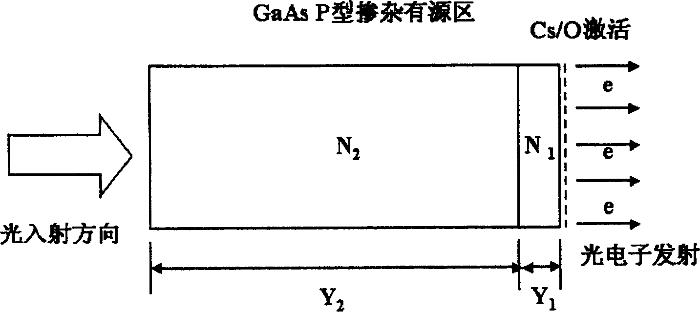
[0026]The transmissive photocathode was fabricated using an inversion process. Since the thickness of the P-type gallium arsenide active region is very thin (about 2 μm), there must be a support body. First, an AlGaAs-GaAs double heterojunction structure was grown on a GaAs substrate by molecular beam epitaxy (MBE) (see Figure 1(a) for a schematic diagram of the growth structure). Then the structure is inverted and heat-sealed on the optical window material, which acts as a support for the active region (see Figure 1(b) for the inversion process). After being inverted and heat-sealed, a series of chemical treatments are carried out to etch away the gallium arsenide substrate all the way to the reaction ba...


PUM


Abstract

This invention relates to semi-conductor material technique used in transparent negative electron affinity gallium arsenide light negative electrode device. This invention source area has two layers of inner layer and surface layer, wherein the inner layer has a window layer outside ad the outside of the surface layer is Se or oxygen actuating layer. The source inner layer is mixed with 1í½8í‡10#+[18]cm#+[-3] in middle concentration and the surface layer is mixed with 5í‡10#+[16]í½1í‡10#+[17]cm#+[-3] in low concentration.

Description

technical field [0001] The invention relates to semiconductor material technology, in particular to a medium-concentration P-type doped transmissive gallium arsenide (GaAs) photocathode material and its preparation technology for transmissive negative electron affinity (NEA) gallium arsenide (GaAs) ) photocathode device. Background technique [0002] At present, the level of my country's development of transmissive negative electron affinity GaAs photocathode devices is: the photoelectric sensitivity can reach 1200μA / lm. There is a big gap between this data and the 3200μA / lm reported internationally. According to the latest report, the minority carrier diffusion length of foreign photocathode materials can reach 7 μm. These data show that, whether it is devices or materials, there is a considerable gap between domestic and foreign countries. [0003] Due to the existence of the surface state and the pinning of the surface energy level, the P-type GaAs material is activate...

Claims


Application Information

Patent Timeline
Patent Type & Authority Applications(China)
IPC IPC(8): H01J1/34H01L21/02H01L33/00
Inventor 王晓峰曾一平
Owner INST OF SEMICONDUCTORS - CHINESE ACAD OF SCI
Why Eureka
Try Eureka