Organic EL element and organic light-emitting device

An organic and component technology, applied in the direction of light-emitting materials, organic dyes, electrical components, etc., can solve problems such as difficult to describe, unable to obtain sufficient hole buffering effect, etc., to suppress the increase of voltage, difficult to voltage, and long driving life. Effect

Inactive Publication Date: 2012-09-26
MITSUBISHI CHEM CORP
View PDF19 Cites 2 Cited by
  • Summary
  • Abstract
  • Description
  • Claims
  • Application Information

AI Technical Summary

Problems solved by technology

[0011] However, there is a problem that a sufficient hole buffering effect cannot be obtained
Furthermore, the scope of application of this invention i

Method used


Image

  • Organic EL element and organic light-emitting device
  • Organic EL element and organic light-emitting device
  • Organic EL element and organic light-emitting device

Examples


Embodiment

[0381] The present invention will be described more concretely by way of examples, but the present invention is not limited to the description of the following examples within the range not exceeding the gist.

[0382] It should be noted that Examples 1 to 3 correspond to the organic EL element A of the present invention or the organic EL element B of the present invention, and Example 4 corresponds to the organic EL element C of the present invention. In addition, Example 5 corresponds to the organic EL element B of the present invention. The organic EL element D.

reference example 1

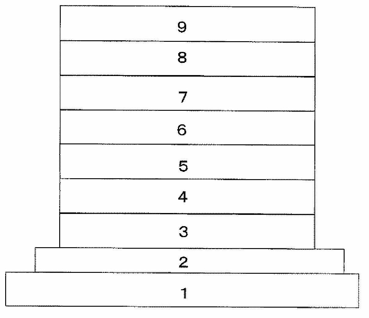
[0384] By the following method to produce a figure 1 An organic EL element of the structure shown.

[0385] (Production of ITO substrate)

[0386] A 150nm indium tin oxide (ITO) transparent conductive film (sputtered film-formed product; sheet resistance 15Ω) was deposited on a glass substrate 1, and patterned into a 2mm wide film using a common photolithography technique and hydrochloric acid etching method. stripes, thereby forming the anode 2.

[0387] (pre-processing)

[0388] The substrate (ITO substrate) on which the anode was patterned as described above was cleaned in the order of ultrasonic cleaning with a surfactant, water washing with pure water, and ultrasonic cleaning with isopropanol, and then it was blown with compressed air. Dry and finally, perform a 1 min UV ozone wash.

[0389] (Film formation of hole injection layer)

[0390] Next, the hole injection layer 3 was formed by a wet film-forming method as follows. 2% by weight of a polymer having a repeat...

reference example 2

[0416] An organic EL element was fabricated in the same manner as in Reference Example 1 except that the hole buffer material HA-1 in Reference Example 1 was changed to BAlq as a hole blocking material shown below.

[0417]


PUM

PropertyMeasurementUnit
Glass transition temperatureaaaaaaaaaa
Film thicknessaaaaaaaaaa

Abstract

Disclosed are: an organic EL element in which a hole is not accumulated in the interface between a light-emitting layer and a cathode-side layer and which has high efficiency and a long service life; and an organic light-emitting device. Specifically disclosed are: an organic EL element comprising an anode, a cathode and a light-emitting layer formed between the anode and the cathode, which is characterized in that the light-emitting layer contains a light-emitting material and a charge transport material, a hole-relaxing layer is formed adjacent to the cathode side of the light-emitting layer, the hole-relaxing layer contains a hole-relaxing material, the hole-relaxing material is an organic compound having a hole-transporting unit and an electron-transporting unit, and at least one charge transport material and at least one hole-relaxing material are the same organic compound as each other; and an organic light-emitting device equipped with the organic EL element.

Description

technical field [0001] The invention relates to an organic EL element with high efficiency and long life and an organic light-emitting device with the element. Background technique [0002] In order to improve the luminous efficiency of an organic EL element, an element using phosphorescence (light emission by triplet excitons) instead of fluorescence (light emission by singlet excitons) has been studied. When phosphorescence is used, the efficiency is considered to be about three times higher than that of devices using fluorescence, and there are reports using europium complexes, platinum complexes, etc. as phosphorescent molecules. However, although conventional organic EL devices using phosphorescent molecules emit light with high efficiency, they are not sufficient for practical use in terms of driving stability, and it is difficult to realize a high-efficiency and long-life display device. [0003] In an organic EL device, light emission is basically obtained by a comb...

Claims


Application Information

Patent Timeline
IPC IPC(8): H01L51/50C09K11/06H05B33/12
CPCC09B57/00C09K2211/1029H05B33/14H01L51/006C09B57/001H01L51/0085H01L51/5096H01L51/0058H01L51/0081C09K11/06H01L51/5048H10K85/626H10K85/633H10K85/324H10K85/342H10K50/14H10K50/18
Inventor 今田一郎五郎丸英贵高桥敦史
Owner MITSUBISHI CHEM CORP
Why Eureka
Try Eureka