Thin film transistor and manufacturing method thereof

A technology of thin film transistors and manufacturing methods, which is applied in the direction of transistors, semiconductor/solid-state device manufacturing, electrical components, etc., and can solve problems affecting the production yield of thin film transistors, metal layer etching residues, and increase of cut-off current of thin film transistors, etc.

Inactive Publication Date: 2012-10-03
CENTURY DISPLAY (SHENZHEN) CO LTD
View PDF9 Cites 9 Cited by
  • Summary
  • Abstract
  • Description
  • Claims
  • Application Information

AI Technical Summary

Problems solved by technology

[0008] However, in this process, after forming the channel layer 130 and the doped semiconductor layer 140, the metal layer 250 is deposited immediately, and the metal atoms in the metal layer 250 are easy to combine with the silicon atoms of the ohmic contact layer 140, thereby increasing the contact resist

Method used


Image

  • Thin film transistor and manufacturing method thereof
  • Thin film transistor and manufacturing method thereof
  • Thin film transistor and manufacturing method thereof

Examples


Embodiment Construction

[0047] In order to make the present invention more comprehensible, preferred embodiments are introduced in detail below. The preferred embodiments of the present invention are provided with corresponding reference numerals in the drawings. In addition, terms such as "first" and "second" in the specification are used to distinguish different elements or processes, rather than to limit their order.

[0048] The present invention will be described in detail below in conjunction with the accompanying drawings and embodiments.

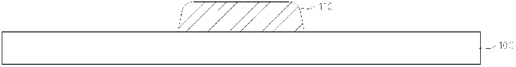
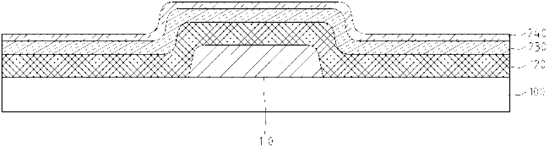
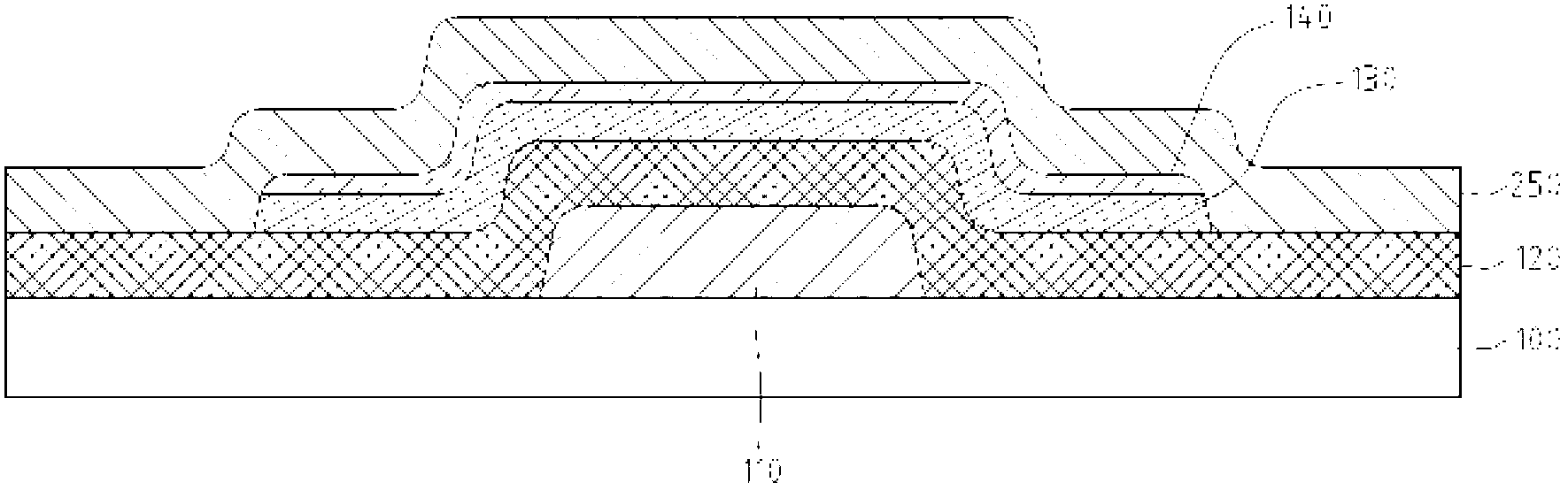
[0049] Please refer to figure 2 , figure 2 It is a flow chart of the manufacturing method of the thin film transistor substrate according to the first embodiment of the present invention. Firstly, step S10 is performed, forming and depositing a first metal layer on the substrate and etching to form a gate. Specifically, a substrate is firstly provided, and a first metal layer is deposited on the substrate, and then the first metal layer is patterned t...


PUM


Abstract

The invention provides a thin film transistor and a manufacturing method thereof. The method comprises the following steps: forming a grid electrode, a grid insulation layer, a semiconductor layer and a doped semiconductor layer on a base plate; nitriding by using plasma, so that Si-N weak bonding on the surface of the doped semiconductor layer; depositing a second metal layer; and etching to form a source electrode and a drain electrode and exposing the semiconductor layer between the source electrode and the drain electrode. The Si-N weak bonding is formed on the doped semiconductor layer before the second metal layer is deposited, so silicon atoms between the second metal layer and the doped semiconductor layer are prevented from forming bonding, contact resistance is reduced, and etching residue caused by reduced etching speed is avoided.

Description

[technical field [0001] The invention relates to a thin film transistor substrate and a manufacturing method thereof. 【Background technique】 [0002] Liquid crystal displays have been widely used in recent years because of their low power consumption, low manufacturing cost, and no radiation. A liquid crystal display generally includes a thin film transistor array substrate, a color filter substrate and a liquid crystal layer sandwiched between the thin film transistor array substrate and the color filter substrate, wherein the thin film transistor is mainly used to control the data writing of the liquid crystal display, It mainly includes components such as gate, channel region, source and drain. [0003] In today's thin film transistor array substrate process, the number of masks used can be reduced to five or four mask processes or even three masks. Taking the general five mask process as an example, the manufacture of thin film transistors accounts for The first three ...

Claims


Application Information

Patent Timeline
IPC IPC(8): H01L29/786H01L21/329
Inventor 许民庆张芳芳李宏远于艳玲
Owner CENTURY DISPLAY (SHENZHEN) CO LTD
Why Eureka
Try Eureka