
Method for manufacturing semiconductor device

A manufacturing method and semiconductor technology, applied in the fields of semiconductor/solid-state device manufacturing, electrical components, circuits, etc., can solve the problems of increased leakage current, dishing of the metal gate surface, and reduced thickness of the metal gate, so as to improve performance , to overcome the residual effect

Active Publication Date: 2012-10-17
SEMICON MFG INT (SHANGHAI) CORP
View PDF4 Cites 2 Cited by
  • Summary
  • Abstract
  • Description
  • Claims
  • Application Information

AI Technical Summary

Problems solved by technology

This will have a great impact on the subsequent process, such as causing an increase in leakage current, etc.
More importantly, it will cause the metal used to form the metal gate to remain in the recess when the metal is filled in the subsequent process to form the metal gate.
In the prior art, an over polishing process is usually used to remove the residual metal in the recess, but it will bring a series of problems such as the reduction of the thickness of the metal gate and the dishing of the surface of the metal gate.

Method used


Image

  • Method for manufacturing semiconductor device
  • Method for manufacturing semiconductor device
  • Method for manufacturing semiconductor device

Examples


Embodiment Construction

[0034] In the following description, numerous specific details are given in order to provide a more thorough understanding of the present invention. It will be apparent, however, to one skilled in the art that the present invention may be practiced without one or more of these details. In other examples, some technical features known in the art are not described in order to avoid confusion with the present invention.

[0035] Now, exemplary embodiments according to the present invention will be described in more detail with reference to the accompanying drawings. These example embodiments may, however, be embodied in many different forms and should not be construed as limited to only the embodiments set forth herein. It should be understood that these embodiments are provided so that this disclosure will be thorough and complete and will fully convey the concept of these exemplary embodiments to those of ordinary skill in the art. In the drawings, the thicknesses of layers a...


PUM


Abstract

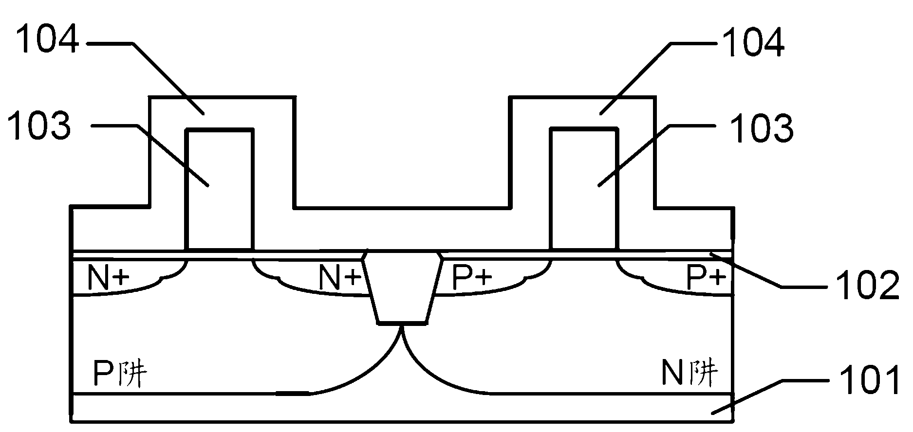
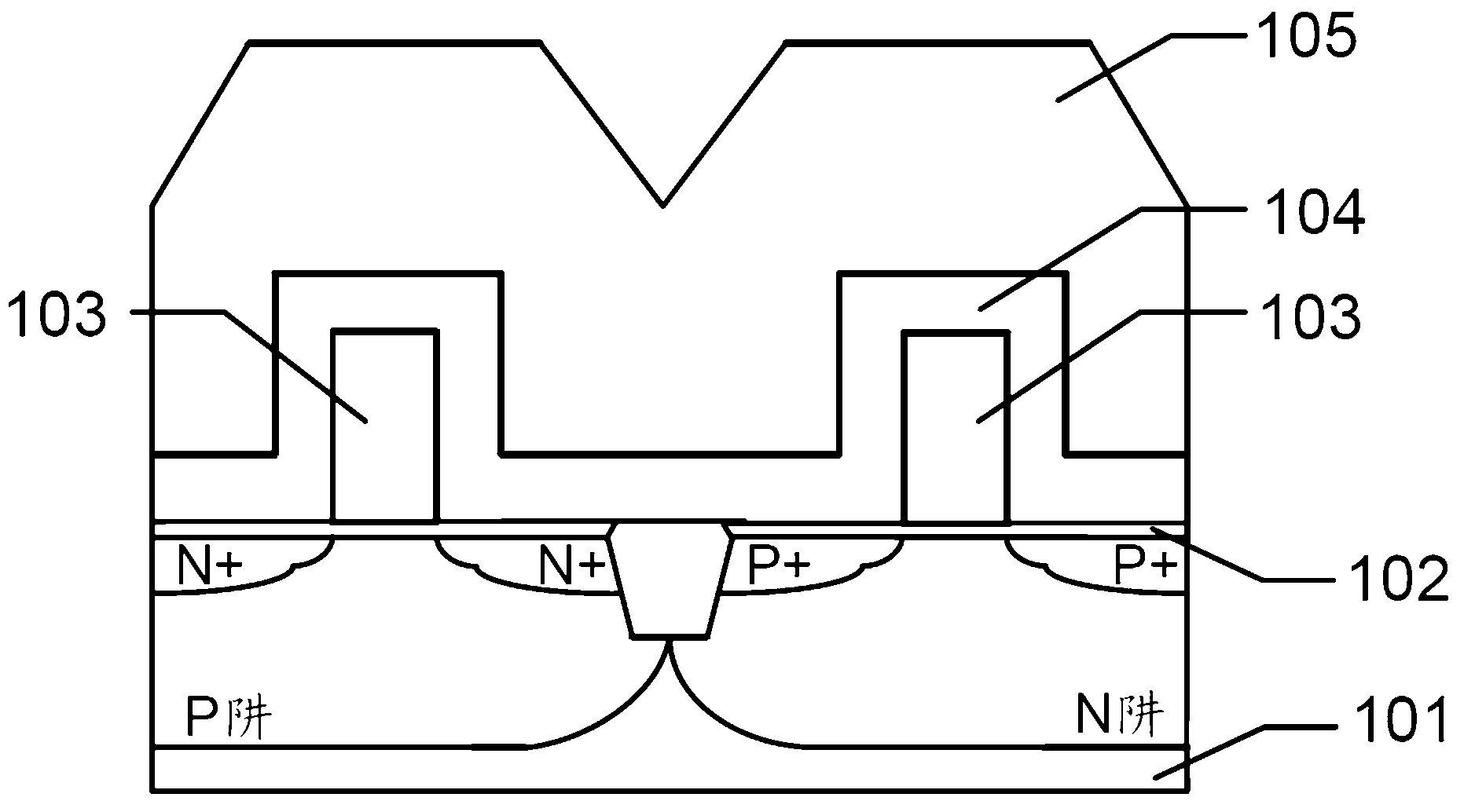
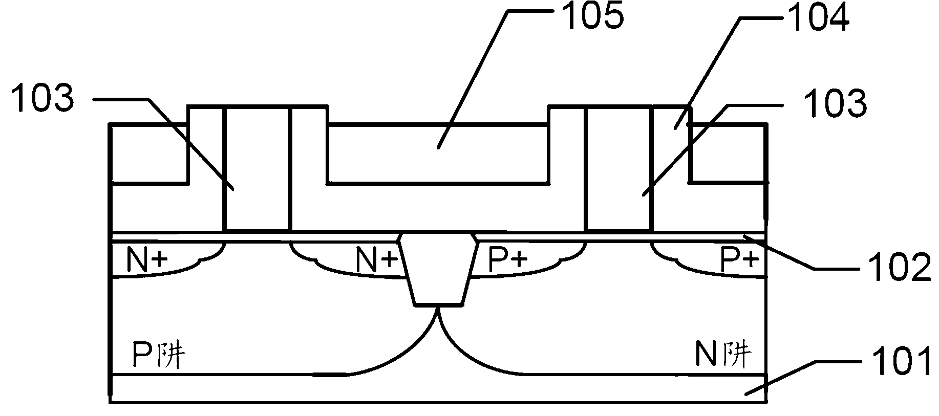
The invention relates to a method for manufacturing a semiconductor device, comprising the steps of: a) providing a substrate, forming a gate dielectric layer on the substrate, forming a dummy gate on the gate dielectric layer, and forming an etch stop layer covering the gate dielectric layer and the dummy gate; b) forming a pre-metal dielectric layer on a front-end device layer structure; c) planarizing the pre-metal dielectric layer until the upper surface of the dummy gate is exposed; d) removing the dummy gate to form an opening for accommodating a metal gate; e) forming a photoresist layer within the opening and on the surface of the pre-metal dielectric layer; f) planarizing the photoresist layer and the protruding etch stop layer; g) removing the photoresist layer within the opening; and h) forming a metal gate within the opening. The method, after the dummy gate is removed, can help effectively reduce dishing phenomenon in dense areas, overcome the defects caused by residue of metal used for forming gates and reduction on the thickness of gates, and improve performance of semiconductor devices.

Description

technical field [0001] The present invention relates to a semiconductor manufacturing process, and more particularly, the present invention relates to a method of manufacturing a semiconductor device with a metal gate. Background technique [0002] The gate usually has the smallest physical dimension in the semiconductor manufacturing process, and its width is usually the most critical critical dimension (CD) on the wafer, so the fabrication of the gate is one of the most critical steps in the process of semiconductor device manufacturing. [0003] Because polysilicon material has the advantages of high temperature resistance and the ability to prevent atoms doped by ion implantation from entering the channel region, polysilicon material is usually used to make the gate of the transistor when making a typical metal oxide semiconductor transistor. However, the polysilicon gate has a relatively high resistance value, which is prone to depletion effect and boron penetration int...

Claims


Application Information

Patent Timeline
Patent Type & Authority Applications(China)
IPC IPC(8): H01L21/336
Inventor 邵群
Owner SEMICON MFG INT (SHANGHAI) CORP
Learn More