
Method for improving write redundancy of high SRAM (static random access memory)

A write-redundant, static-random technology used in semiconductor/solid-state device manufacturing, electrical components, circuits, etc.

Active Publication Date: 2014-09-03
SHANGHAI HUALI MICROELECTRONICS CORP
View PDF12 Cites 0 Cited by
  • Summary
  • Abstract
  • Description
  • Claims
  • Application Information

AI Technical Summary

Problems solved by technology

[0005] The purpose of the present invention is to provide a method for improving the write redundancy of SRAM, so as to solve the problem that the source and drain of PMOS devices and pull-up tubes in ordinary processes will not form a silicon carbide lattice structure

Method used


Image

  • Method for improving write redundancy of high SRAM (static random access memory)
  • Method for improving write redundancy of high SRAM (static random access memory)
  • Method for improving write redundancy of high SRAM (static random access memory)

Examples


Embodiment approach

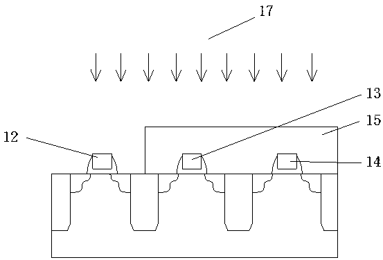
[0022] In the first embodiment of the present invention, please continue to refer to Figure 4a and Figure 4b shown. The above-mentioned lattice structure 18 is specifically a silicon carbide lattice structure. After the carbon implantation 17 process is performed, the source and drain ends of the NMOS device 12 and the source and drain ends of the pull-up tube 14 form a silicon carbide lattice structure.

[0023] In the second embodiment of the present invention, the above-mentioned covering layer 15 is photoresist.

[0024] In the third embodiment of the present invention, after carbon implantation 17 is performed on the NMOS device 12, the PMOS device 13 and the pull-up tube 14, an annealing process is required to finally make the source and drain ends of the NMOS device 12 and the pull-up tube 14 The source-drain two-terminal silicon carbide lattice structure.

[0025] To sum up, using the method of the present invention to improve the writing redundancy of the SRAM, ...


PUM


Abstract

The invention discloses a method for improving the writing redundancy of static random access memory, which includes an NMOS device with a covering layer, a PMOS device and a pull-up tube. First, the covering layer on the NMOS device and the pull-up tube is simultaneously Remove, and then perform carbon implantation on the NMOS device, the PMOS device with the overlay and the pull-up tube, so that the source and drain ends of the NMOS device and the source and drain ends of the pull-up tube form a lattice structure , to increase the tensile stress in the channel direction. Using a method of improving the write redundancy of static random access memory according to the present invention, by adopting a carbon injection process for the source and drain of the pull-up tube, the tensile stress of the pull-up tube in the channel direction is enhanced, and the pull-up tube device is effectively reduced The carrier mobility increases, the equivalent resistance of the pull-up tube is increased, and at the same time, the random memory writing redundancy is improved.

Description

technical field [0001] The invention relates to the technical field of semiconductor preparation, in particular to a method for improving the writing redundancy of a SRAM. Background technique [0002] Static random access memory (SRAM), as an important product in semiconductor memory, has been widely used in high-speed data exchange systems such as computers, communications, and multimedia. figure 1 For a typical SRAM cell layout below 90nm, see figure 1 shown. It includes three levels of active region 4 , polysilicon gate 5 and contact hole 6 . The control tube 1 (Pass Gate) area is an NMOS device, the pull down tube (Pull Down MOS) 2 area is also an NMOS device, and the pull up tube (Pull Up MOS) 3 area is a PMOS device. [0003] Write margin (Write Margin) is an important parameter to measure the write performance of SRAM cells. figure 2 For the working schematic diagram of SRAM device when writing, please refer to figure 2 shown. Assuming that node 7 stores data...

Claims


Application Information

Patent Timeline
Patent Type & Authority Patents(China)
IPC IPC(8): H01L21/8244H10B10/00
Inventor 俞柳江
Owner SHANGHAI HUALI MICROELECTRONICS CORP
Learn More