Alignment mark structure of medium substrate zero layer

A technology of zero-layer alignment marks and dielectric substrates, which is applied in the fields of optics, instruments, and photoplate-making on patterned surfaces, etc., can solve problems such as inconvenient alignment, easy confusion, and difficulty in searching for alignment marks, and achieves easy Search, easy alignment effects

Inactive Publication Date: 2012-10-24
THE 41ST INST OF CHINA ELECTRONICS TECH GRP
View PDF0 Cites 1 Cited by
  • Summary
  • Abstract
  • Description
  • Claims
  • Application Information

AI Technical Summary

Problems solved by technology

[0007] (1) The alignment mark is a circular through hole, and it is inconvenient to align through the handwheel movement in the X and Y directions;
[0008] (2) During photolithography alignment, since the position of the alignment mark is not special, it is difficult to search for the alignment mark, which affects work efficiency;
[0009] (3) The structure of the alignment mark is the same as that of other through-hole arrays, which is easy to confuse. Once confused, it will be reworked if it is light, and the yield will be affected if it is serious;

Method used


Image

  • Alignment mark structure of medium substrate zero layer
  • Alignment mark structure of medium substrate zero layer
  • Alignment mark structure of medium substrate zero layer

Examples


Embodiment 1

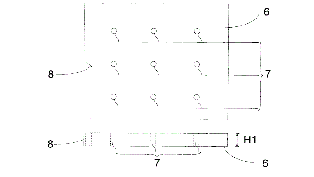
[0029] See figure 2 The zero-layer alignment mark structure 8 of the dielectric substrate is a longitudinal through hole arranged at the edge of the dielectric substrate 6 and is a right triangle. In this embodiment, the dielectric substrate 6 where the zero-layer alignment mark structure 8 of the dielectric substrate is located is made of 99.6% or more alumina ceramics, the plane size is 5.08 mm×5.08 mm, and the thickness H1 is 0.635 mm.

Embodiment 2

[0031] See image 3 The zero-layer alignment mark structure 9 of the dielectric substrate is a longitudinal through hole provided on the edge of the dielectric substrate 6 and is a rectangle. In this embodiment, the dielectric substrate 6 where the zero-layer alignment mark structure 9 of the dielectric substrate is located is made of 99.6% or more alumina ceramics, the plane size is 5.08 mm×5.08 mm, and the thickness H2 is 0.254 mm.

Embodiment 3

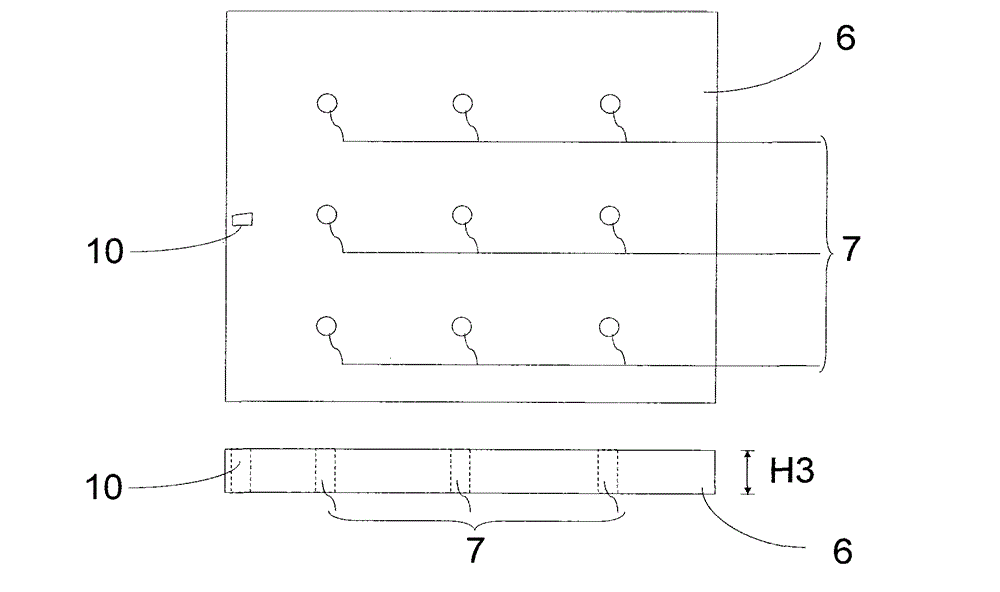
[0033] See Figure 4 The zero layer alignment mark structure 10 of the dielectric substrate is a longitudinal through hole arranged on the edge of the dielectric substrate 6 and is a right-angled trapezoid. In this embodiment, the dielectric substrate 6 where the zero-layer alignment mark structure 10 of the dielectric substrate is located is made of sapphire, the plane size is 5.08 mm×5.08 mm, and the thickness H3 is 0.508 mm.

[0034] In the manufacturing process of microwave thin film hybrid integrated circuits, use Figure 2 to Figure 4 The zero-layer alignment mark structures 8, 9, and 10 of the dielectric substrate can ensure that the microwave thin film hybrid integrated circuit on the dielectric substrate is manufactured at its preset position.

[0035] To sum up, the zero-layer alignment mark structure of the dielectric substrate of the present invention is a right-angled longitudinal through hole arranged on the edge of the dielectric substrate, which can ensure that the ...


PUM

PropertyMeasurementUnit
thicknessaaaaaaaaaa
sizeaaaaaaaaaa
thicknessaaaaaaaaaa

Abstract

An alignment mark structure of a medium substrate zero layer is a right-angle-type longitudinal through hole arranged at an edge of the medium substrate, and can be a right-angled triangle, a rectangle and a right-angled trapezoid. Materials of the medium substrate on which the alignment mark structure of the medium substrate zero layer is located comprise more than 99.6% of alumina ceramic and sapphire, and the medium substrate has a thickness of 0.1 to 0.65 mm. According to the alignment mark structure, not only can the aligning precision be ensured when photoetching of multilayer metal film is performed on the medium substrate containing micro array through holes, but also the yield of microwave film integrated circuit can be improved.

Description

Technical field [0001] The invention relates to a zero-layer alignment mark structure of a dielectric substrate, in particular to an alignment mark related to a photoetching device in the field of manufacturing microwave thin film hybrid integrated circuits or other micro-devices. Background technique [0002] In the microwave frequency band, many circuits need to be directly grounded, and the metallization of small through holes is a good grounding method. Its purpose is to reduce grounding inductance and shorten the heat transfer path, which is particularly important for microwave and millimeter wave device and circuit design. Therefore, tiny metallized vias have become a common passive component of microwave and millimeter wave integrated circuits, and the shape of the vias is usually circular. [0003] The microwave thin film hybrid integrated circuit is processed by the large substrate of the semiconductor integrated circuit and the multi-unit method, which has high productio...

Claims


Application Information

Patent Timeline
Patent Type & Authority Applications(China)
IPC IPC(8): G03F9/00
Inventor 曹乾涛
Owner THE 41ST INST OF CHINA ELECTRONICS TECH GRP
Why Eureka
Try Eureka