Method for fabricating a semiconductor power device

A technology of power semiconductors and manufacturing methods, which is applied in semiconductor/solid-state device manufacturing, semiconductor devices, transistors, etc., can solve problems such as incomplete contact of contact surfaces, uneven junctions in depletion regions, and reduction of super interface withstand voltage capacity, etc., to achieve The effect of improving the pressure resistance

Inactive Publication Date: 2012-10-24
ANPEC ELECTRONICS CORPORATION
View PDF6 Cites 0 Cited by
  • Summary
  • Abstract
  • Description
  • Claims
  • Application Information

AI Technical Summary

Problems solved by technology

For example, by the above method of etching the epitaxial layer, a flat surface cannot be produced on the sidewall of the trench, so the contact surface between the first conductivity type epitaxial layer and the second conductivity type epitaxial layer cannot be a flat surface, and even the first conductivity type epitaxial layer cannot be flat. Type epitaxial layer and the contact surface of the second conductivity type epitaxial layer will have incomplete contact
Causes the junction of the depletion region produced by the epitaxial layer of the first conductivity type and the epitaxial layer of the second conductivity type to be uneven, further reducing the withstand voltage capability of the super interface

Method used


Image

  • Method for fabricating a semiconductor power device
  • Method for fabricating a semiconductor power device
  • Method for fabricating a semiconductor power device

Examples


Embodiment Construction

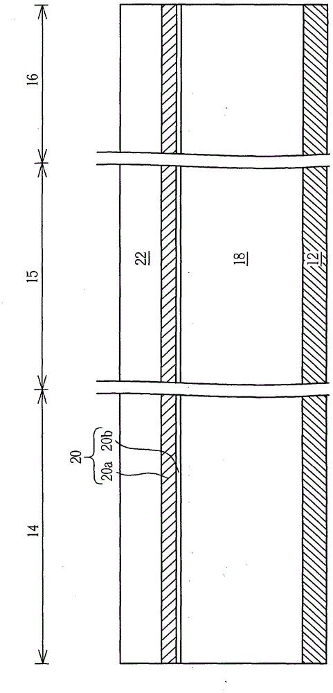
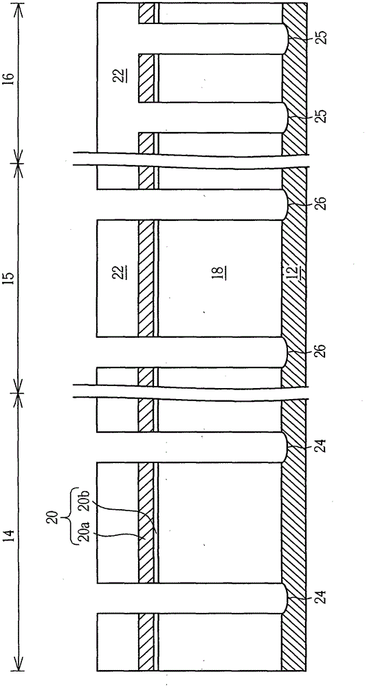
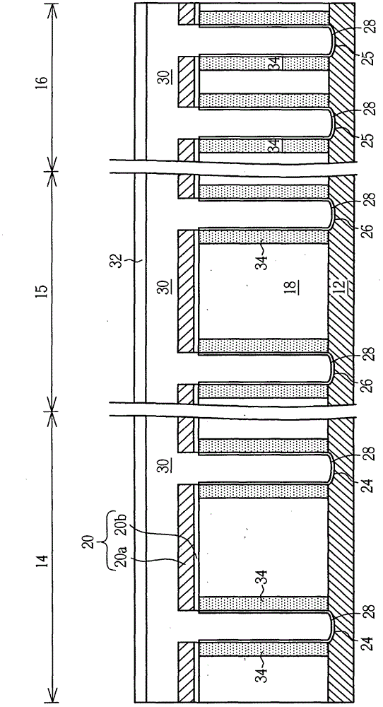
[0030] Please refer to Figure 1 to Figure 16 , which is characterized in that the manufactured power device may include trench power MOSFETs, and the same devices or parts in the drawings are represented by the same symbols. It should be noted that the drawings are for illustration only and are not to scale.

[0031] Please refer to figure 1 Firstly, a substrate 12 of the first conductivity type is provided, and the substrate 12 of the first conductivity type is an N+ type doped silicon substrate, which can be regarded as a drain of a power MOSFET. A cell region (cell region) 14 is defined on the substrate 12 of the first conductivity type, a peripheral voltage-resistant region (termination region) 16 surrounding the cell region 14, and a termination region (termination region) 16 disposed between the cell region 14 and the peripheral voltage-resistant region 16 are defined. The transition region (transition region) 15 is characterized in that the transistor device with swi...


PUM

PropertyMeasurementUnit
thicknessaaaaaaaaaa

Abstract

The present invention provides a method for fabricating a power device. A first conductive substrate is provided, and a conductive epitaxial layer is formed on conductive substrate substrate. Then a pad layer and a hard mask are formed on the first conductive epitaxial layer. At least a trench is etched into the hard mask, the pad layer, and the first conductive epitaxial layer. The hard mask is removed and a buffer layer is formed at the sidewall of the trench. The trench is then filled with a dopant source layer comprising plural dopants. A drive-in process is performed to diffuse the second conductive dopants into the first conductive epitaxial layer through the buffer layer, thereby forming a second conductive diffusion region.

Description

technical field [0001] The invention relates to the technical field of power semiconductor devices, in particular to a method for manufacturing a power metal oxide semiconductor field-effect transistor (power MOSFET) device with a super-junction. Background technique [0002] Power semiconductor devices are often used in power management, such as switching power supply, computer center or peripheral power management IC, backlight power supply or motor control, etc., and its types include insulated gate bipolar transistors (insulated gate bipolar transistor (IGBT), metal-oxide-semiconductor field effect transistor (MOSFET) and bipolar junction transistor (bipolar junction transistor, BJT) and other devices. Among them, MOSFETs are widely used in various fields because they can save power and provide faster device switching speeds. [0003] In a power device, the design of the substrate is that P-type epitaxial layers and N-type epitaxial layers are arranged alternately, so t...

Claims


Application Information

Patent Timeline
Patent Type & Authority Applications(China)
IPC IPC(8): H01L21/336
CPCH01L27/088H01L29/41766H01L29/456H01L29/66727H01L29/1095H01L29/0619H01L21/2255H01L29/7811H01L29/0634
Inventor 林永发徐守一吴孟韦陈面国詹景晴石逸群
Owner ANPEC ELECTRONICS CORPORATION
Why Eureka
Try Eureka