

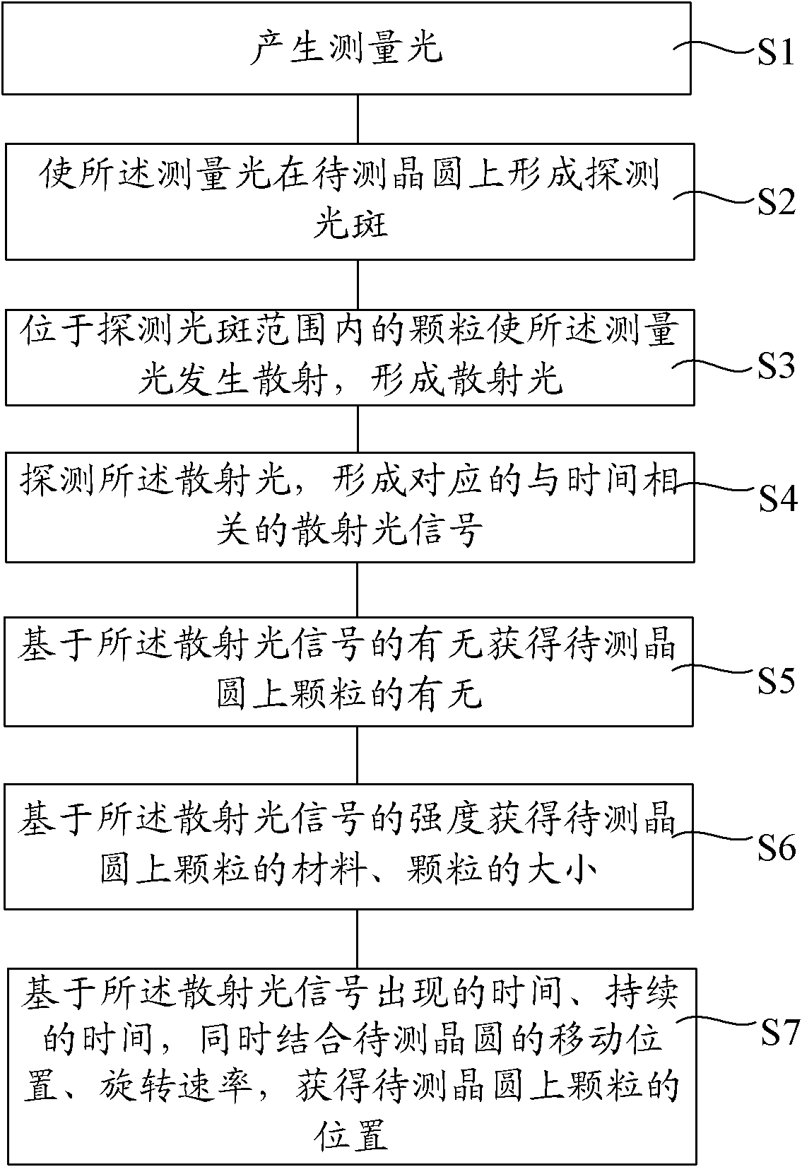
Wafer detecting method and wafer detecting device
A detection method and detection device technology, applied in the field of semiconductors, can solve problems affecting detection accuracy, large DOE volume, and reduced signal strength, and achieve the effects of simplifying the detection light system, increasing the detection rate, and improving the detection accuracy
- Summary
- Abstract
- Description
- Claims
- Application Information
AI Technical Summary
Problems solved by technology
Method used
Image

Examples
Embodiment Construction
[0025] In the following description, numerous specific details are set forth in order to provide a thorough understanding of the present invention. However, the present invention can be implemented in many other ways different from those described herein, and those skilled in the art can make similar promotions without departing from the connotation of the present invention. Therefore, the present invention is not limited by the specific implementation disclosed below.
[0026] Next, the present invention is described in detail by using schematic diagrams. When describing the embodiments of the present invention in detail, for the convenience of description, the schematic diagrams are only examples, which should not limit the protection scope of the present invention.
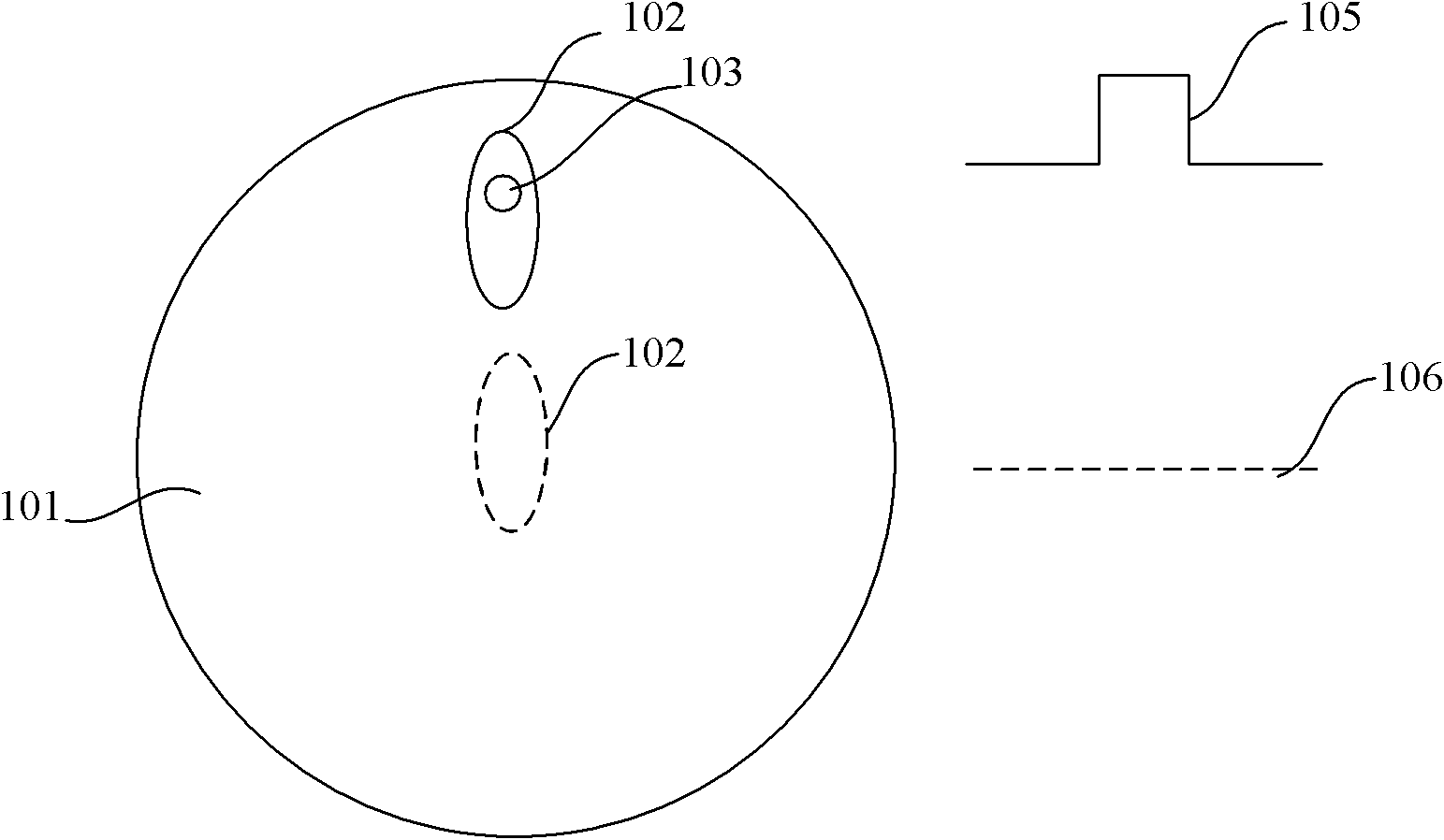
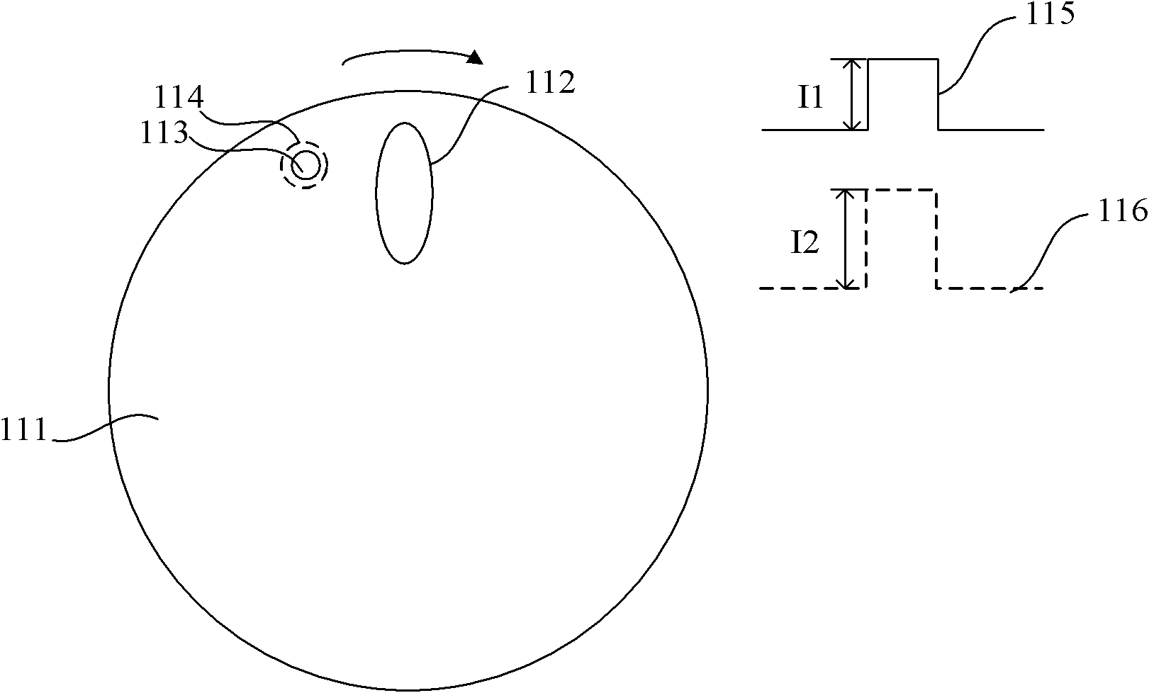
[0027] The specific embodiments of the present invention will be described in detail below with reference to the accompanying drawings. The invention provides a wafer detection method, comprising: generating me...
PUM
| Property | Measurement | Unit |
|---|---|---|
| Diameter | aaaaa | aaaaa |
Abstract
Description
Claims
Application Information