High-density PCB

A high-density, solder pad technology, which is applied in the direction of electrical connection of printed components, printed circuit components, and assembly of printed circuits with electrical components, can solve the problems of difficult layout of solder pads on printed boards, pin adhesion, and high scrap rate. Reach the effect of reducing sticking rate, improving yield and reducing solder fluid

Inactive Publication Date: 2012-10-31
秦玉成
View PDF3 Cites 3 Cited by
  • Summary
  • Abstract
  • Description
  • Claims
  • Application Information

AI Technical Summary

Problems solved by technology

[0004] The display screen with in-line LED lights basically uses RGB (R red, G green, and B blue) three LED lights or RGBW (R red, G green, B blue, W white) four LED lights Composed of lights, a single pixel requires multiple monochromatic LEDs to display together, and it is difficult for the display to achieve high density
[0005] The t

Method used


Image

  • High-density PCB
  • High-density PCB
  • High-density PCB

Examples


Example Embodiment

[0026] Hereinafter, the present invention will be further described in detail through specific embodiments in conjunction with the accompanying drawings.

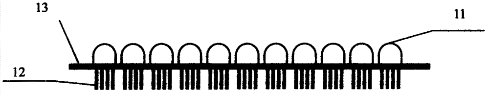
[0027] Such as figure 1 As shown, the three-in-one LED lamp 11 has 4 pins. In the LED display application scenario, a large number of components are arranged on the PCB board 13. The density of the pins 12 of the device is very high. During the processing, Especially when wave soldering is used, solder often sticks between the pins, resulting in a very low yield of product production, and large-scale production cannot be carried out. This is particularly prominent in the production process of LED displays.

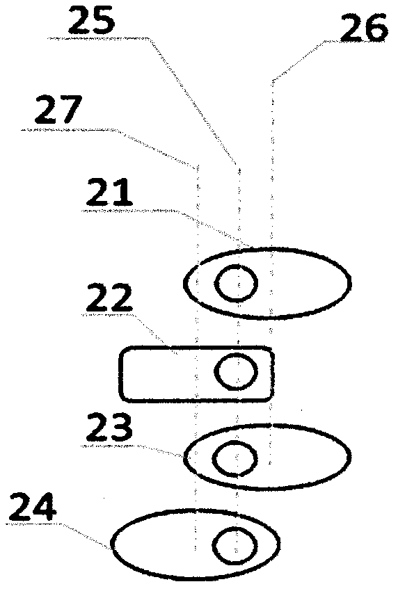
[0028] Such as figure 2 , A specific implementation technical solution of the present invention to solve the technical problem, the center line 26 or 27 of the set pad is not in a straight line with the center 25 of the solder hole, and the centers of adjacent pads are located on both sides of the center line of the solder h...


PUM


Abstract

The invention discloses a structure and a manufacturing method of a high- density PCB, and further discloses a DIP (Double In-line Package) LED display adopting the high-density PCB. The manufacturing method of the high-density PCB comprises the following steps: adjacent bonding pads are respectively mounted at the center line position deviated from welding holes, at which diversion pads are arranged. By adopting the method provided by the invention, pins are not adhered when the high-density PCB is subject to wave soldering and solder impact during manufacturing. The high-density PCB is suitable for large-scale industrial production and application.

Description

Technical field [0001] The invention relates to an LED display screen, particularly a direct-plug LED lamp display screen. Background technique [0002] LED (light emitting diode, LED for short). It is a way to display characters by controlling the on and off of semiconductor light-emitting diodes. A display screen used to display various information such as text, graphics, images, animation, quotation, video, and video signals. [0003] LED (light emitting diode, abbreviated as LED) display screen, is composed of LED dot matrix, through the red, blue, green LED lights to display text, pictures, animation, video, the content can be replaced at any time, each part The components are all display devices with a modular structure. Usually composed of display module, control system and power supply system. [0004] The display screen with direct plug-in LED lights basically uses RGB (R red, G green, and B blue) LED lights or uses RGBW (R red, G green, and B blue, W white) four LEDs I...

Claims


Application Information

Patent Timeline
IPC IPC(8): H05K1/11H05K3/32
Inventor 秦玉成
Owner 秦玉成
Why Eureka
Try Eureka