DDS (data-data short) detection structure and DDS detection method
A technology for detecting structures and on-off switches, applied in nonlinear optics, instruments, optics, etc., can solve the problems of increased analysis time, cumbersome analysis process, and inability to confirm the cause of defects more effectively and timely, so as to improve product yield Effect
- Summary
- Abstract
- Description
- Claims
- Application Information
AI Technical Summary
Problems solved by technology
Method used
Image
Examples
Embodiment 2
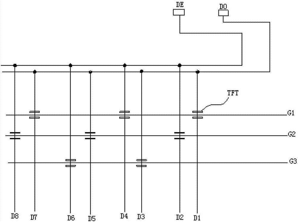
[0034] Such as figure 2 As shown, this embodiment is an example extended on the basis of Embodiment 1. The on-off switch in this embodiment is a thin film field effect transistor (TFT) switch TFT, and the detection structure also includes controlling the TFT The control line for switching TFT on and off.
[0035] In this embodiment, the control lines are fabricated on the same layer as the gate lines on the display panel.
[0036] The detection structure is provided with at least N control lines, and N is greater than or equal to 3 and less than or equal to the total number of data lines; the thin film field effect transistor switches TFTs on each sequentially arranged N data lines are respectively controlled by different control lines.
[0037] Such as figure 2 As shown, there are three control lines in this embodiment, namely the first control line G1, the second control line G2 and the third control line G3. Depend on figure 2 It can be seen that the first control li...
Embodiment 3
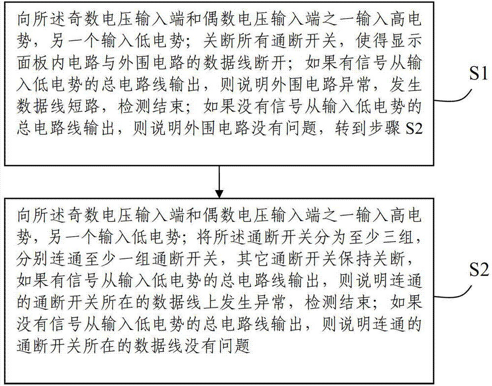
[0039] Such as image 3 As shown, this embodiment describes a method for DDS detection using the DDS detection structure described in Embodiment 1 or Embodiment 2, including the following steps:
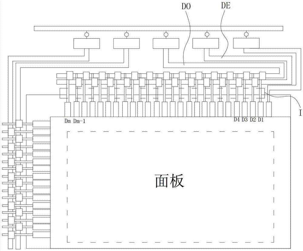
[0040] S1: Input a high potential to one of the odd-numbered voltage input terminals and even-numbered voltage input terminals, and input a low potential to the other; turn off all the on-off switches, so that the data lines of the circuit in the display panel and the peripheral circuit are disconnected; if there is a signal Output from the main circuit line with input low potential indicates that the peripheral circuit is abnormal, the data line is short-circuited, and the detection is over; if no signal is output from the main circuit line with low potential input, it means that there is no problem with the peripheral circuit, and go to step S2;
[0041]S2: Input a high potential to one of the odd-numbered voltage input terminals and even-numbered voltage input terminals, and input...
Embodiment 4
[0044] This embodiment is an example extended on the basis of Embodiment 3, specifically when the DDS detection structure described in Embodiment 2 is used for DDS detection:
[0045] First, a high potential is input to the odd voltage input terminal of the odd total circuit line DO, and a low potential is input to the odd voltage input terminal of the even total circuit line DE, and at this time the first control line G1, the second control line G2 and the third control line G3 all input low voltage, that is, at this time all the thin film field effect transistor switches TFT on the data line are disconnected, if there is a signal output from the even total circuit line DE, it means that there is SD metal in the peripheral circuit (the metal of the data line Material) remains, causing two adjacent data lines to be turned on, resulting in a short circuit. If no signal is output from the even bus line DE, it means that there is no problem with the peripheral circuit. After the ...
PUM
 Abstract
Description
Claims
Application Information


