Differential capacitive micro-acceleration transducer and manufacturing method thereof

A technology of micro-acceleration and differential capacitance, which is applied in the direction of measurement of acceleration, velocity/acceleration/shock measurement, piezoelectric device/electrostrictive device, etc. It can solve the problems of complex test methods, avoid repeated photolithography, small stiffness, The effect of improving sensitivity

Active Publication Date: 2012-11-14
SHANGHAI INST OF MICROSYSTEM & INFORMATION TECH CHINESE ACAD OF SCI
View PDF2 Cites 22 Cited by
  • Summary
  • Abstract
  • Description
  • Claims
  • Application Information

AI Technical Summary

Problems solved by technology

[0009] In view of the above-mentioned shortcomings of the prior art, the object of the present invention is to provide a differential capacitance micro-acceleration sensor and its manufacturing method, which is used to solve the non-linearity of capacitance change in the prior art and the test caused by the small capacitance change caused by acceleration. complex problem

Method used


Image

  • Differential capacitive micro-acceleration transducer and manufacturing method thereof
  • Differential capacitive micro-acceleration transducer and manufacturing method thereof
  • Differential capacitive micro-acceleration transducer and manufacturing method thereof

Examples


Embodiment 1

[0074] Such as Figures 1a to 1i As mentioned above, this embodiment provides a method for manufacturing a differential capacitive micro-acceleration sensor, comprising the following steps:

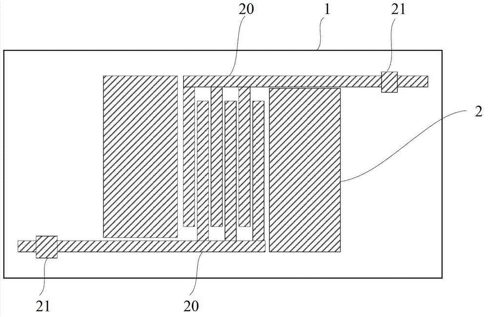
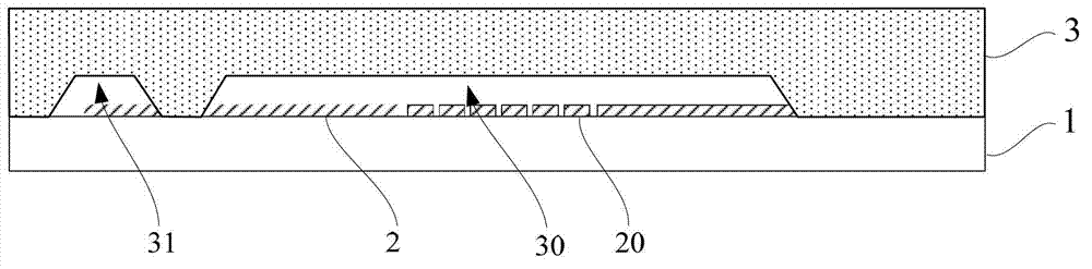
[0075] Step S1: if Figure 1a As shown, a glass substrate 1 is provided, and a metal layer 2 is evaporated or deposited on the front side of the glass substrate 1 by electron beams. The material of the metal layer 2 is tentatively selected as Au, but it is not limited thereto. In other In the embodiment, it can also be a conductive metal such as Al, Cu, or Ag; then, a pair of interdigitated fixed electrodes 20 and two fixed electrode contacts 21 are produced by performing photolithography and etching on the metal layer 2 .

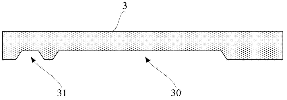
[0076] Step S2: Provide a structural substrate 3. In this embodiment, the structural substrate is temporarily selected as a silicon wafer, but it is not limited thereto. In other embodiments, it can also be other substrates, and different structural substrate process...

Embodiment 2

[0088] As shown in Figures 2a to 2e, they are part of the process flow chart for making a differential capacitive micro-acceleration sensor in this embodiment. This embodiment provides another method for manufacturing a differential capacitive micro-acceleration sensor, which is different from the first embodiment. The substrate provided in this embodiment is a silicon substrate, therefore, the difference in the substrate leads to a slight difference in the process, and the specific process steps are as follows:

[0089] When a silicon substrate 1 is provided, step S1 of the first embodiment further includes:

[0090] S1-1: If Figure 2a As shown, a substrate 1 is provided, and a silicon oxide layer 9 is thermally oxidized and grown on the front side of the silicon substrate, and the silicon oxide layer 9 insulates the silicon substrate from the metal layer 2 in subsequent steps.

[0091] S1-2: If Figure 2b As shown, a layer of metal layer 2 is prepared on the silicon oxide...

Embodiment 3

[0098] As shown in Figures 3a to 3d, it is a partial process flow chart of making a differential capacitive micro-acceleration sensor in this embodiment. This embodiment provides another method for manufacturing a differential capacitive micro-acceleration sensor, which is different from the first embodiment. The structural substrate provided in this embodiment is an SOI substrate. Therefore, the difference in the structural substrate also leads to a slight difference in the process. The specific process steps are as follows:

[0099] When providing an SOI structure substrate 3, step S2 of the first embodiment further includes:

[0100] S2-1: If Figure 3a As shown, a structural substrate 3 is provided, and a layer of silicon oxide 9 is thermally oxidized and grown on the surface of the top layer silicon 36 on the back of the structural substrate 3 .

[0101] S2-2: If Figure 3b As shown, photolithography and etching are carried out on the silicon oxide layer 9 on the back s...


PUM


Abstract

The invention discloses a differential capacitive micro-acceleration transducer and a manufacturing method thereof. According to the method, the manufacturing of a movable mass block and an elastic beam is completed by using a bulk-silicon process, and the structure manufacturing and the releasing of a device structure are simultaneously completed by using a dry etching method; a movable electrode and the movable mass block are same in shape and size, so that an operation of repeated photoetching is avoided, thereby greatly simplifying the process; the stiffness of the designed elastic beam is small in the sensitive direction and large in the sensitive vertical direction, therefore, the elastic beam is higher in selectivity and anti-crosstalk capacity; and a device is simply and reliably packaged by using a wafer-level low-temperature vacuum aligned-bonding technology, thereby facilitating the large-scale manufacturing of the device. In addition, the differential capacitive micro-acceleration transducer disclosed by the invention adopts a variable-area type operating principle, so that the movable mass block is only damped by a sliding membrane in the process of moving, thereby improving the sensitivity.

Description

technical field [0001] The invention relates to an acceleration sensor, in particular to a grid-like structure differential capacitive micro-acceleration sensor with a simple manufacturing method and a device size as small as millimeters and a manufacturing method thereof, belonging to the field of microelectronic machinery manufacturing. Background technique [0002] Miniature acceleration sensors are widely and deeply used in aerospace guidance, vehicle control, robotics, mobile phone intelligence, industrial prospecting, medicine and other fields due to their small size, light weight, low power consumption, low cost, and easy integration. In order to adapt to the limitations of measurement conditions in different fields, there are various types of acceleration sensors, but capacitive acceleration sensors have always been the most important research direction because of their good temperature characteristics, high sensitivity, high stability, and simple processing. [0003...

Claims


Application Information

Patent Timeline
Patent Type & Authority Applications(China)
IPC IPC(8): G01P15/125B81C1/00B81B3/00
Inventor 熊斌徐铭徐德辉姚邵康马颖蕾王跃林
Owner SHANGHAI INST OF MICROSYSTEM & INFORMATION TECH CHINESE ACAD OF SCI
Why Eureka
Try Eureka