Longitudinal power device for low-ratio on-resistance employing groove structure with high dielectric constant

A technology with high dielectric constant and specific on-resistance, applied in semiconductor devices, electrical components, circuits, etc., can solve the problems of application limitation, accumulation effect limitation, low constant, etc., and achieve the effect of increasing carrier concentration

Active Publication Date: 2012-11-14
UNIV OF ELECTRONICS SCI & TECH OF CHINA
View PDF5 Cites 25 Cited by
  • Summary
  • Abstract
  • Description
  • Claims
  • Application Information

AI Technical Summary

Problems solved by technology

However, due to the low dielectric constant of silicon dioxide, the effect of the accumulation effect is limited, and too thin silicon dioxide dielectric is likely to cause breakdown of the device gate, so its application is limited

Method used


Image

  • Longitudinal power device for low-ratio on-resistance employing groove structure with high dielectric constant
  • Longitudinal power device for low-ratio on-resistance employing groove structure with high dielectric constant
  • Longitudinal power device for low-ratio on-resistance employing groove structure with high dielectric constant

Examples


Embodiment 1

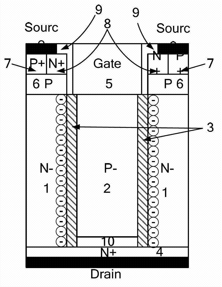
[0030] see figure 1 . In this embodiment, N+ is used as the silicon substrate 4 , N− is used as the drift region 1 , and P− is used as the second filling material 2 inside the high dielectric constant column. In addition, it also includes a P-type doped channel region 6, an ohmic contact heavily doped region 7, a source 8, a polysilicon gate 5, a silicon dioxide insulating gate dielectric 9, a high dielectric constant material column 3, and an isolation insulating dielectric 10, and the isolation insulating medium 10 is located at the bottom of the high dielectric constant column. 10 may use the same material as the high dielectric constant material column 3, or other insulating materials.

[0031] When the device is in the off state, although there are high dielectric constant material columns 3, the alternation of the drift region 1 and the second filling material 2 will still produce the charge balance of the Super Junction, and the introduction of the high dielectric ma...

Embodiment 2

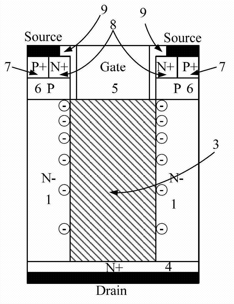
[0033] see figure 2 . In this embodiment, N+ is used as the silicon substrate 4 , N− is used as the drift region 1 , and P− is used as the second filling material 2 of the high dielectric constant column. In addition, it also includes P-type doped channel region 6 , ohmic contact heavily doped region 7 , source 8 , polysilicon gate 5 , silicon dioxide insulating gate dielectric 9 , and high dielectric constant material pillar 3 . At the same time, the same material as the high dielectric constant material column 3 is used as the internal filling and isolation insulating medium 10 , that is, the solid high dielectric constant material column 3 . According to the Poisson equation: the slope of the electric field distribution in the N-drift region satisfies: qN D / ε, and in this embodiment, the high dielectric constant occupies a larger proportion of the drift region, so the average dielectric constant ε in the drift region is larger than that of embodiment 1. Although there ...

Embodiment 3

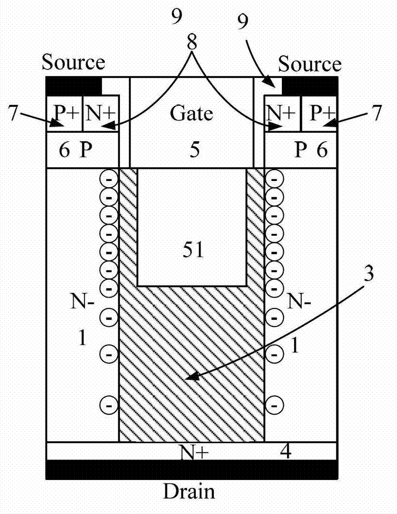
[0035] see image 3 . In this embodiment, N+ is used as the silicon substrate 4 , N− is used as the drift region 1 , and P− is used as the second filling material 2 inside the high dielectric constant column. In addition, it also includes a P-type doped channel region 6, an ohmic contact heavily doped region 7, a source electrode 8, a polysilicon gate 5, a silicon dioxide insulating gate dielectric 9, a high dielectric constant material column 3, and an isolation dielectric 10 located at The bottom of the high dielectric constant pillar. Use the same high dielectric constant material column 3 as the filling material for the lower half of the high dielectric constant column to achieve isolation, and use the material of the gate 5 (polysilicon or metal) as the high dielectric constant material column 3 The top half is filled with material. This embodiment also only uses the electric field modulation effect of the high dielectric material to optimize the distribution of the el...


PUM


Abstract

The invention discloses a longitudinal power device for low-ratio on-resistance employing a groove structure with a high dielectric constant and relates to semiconductor power devices. The longitudinal power device comprises a drift region, a silicon substrate, a gate, a channel region, an ohmic contact heavily-doped region, a source and an insulated gate medium. The longitudinal power device is characterized in that the drift region, the silicon substrate and the source form a first conductive type; the channel region and the ohmic contact heavily-doped region form a second conductive type; a material column with a high dielectric constant is arranged between the gate and the silicon substrate; the gate is directly contacted with the material column with the high dielectric constant; and the drift region surrounds the material column with the high dielectric constant. Compared with a longitudinal Super Junction power device, the low-ratio on-resistance for the high dielectric material power device has the advantage that the reduction in three levels of magnitude exists.

Description

technical field [0001] The invention relates to a semiconductor power device, especially a material and a structure of a pressure-resistant region of a vertical high-voltage device. Background technique [0002] As we all know, traditional vertical power devices withstand high voltage through a layer of low-doped semiconductor drift region. For example, the most typical vertical double-diffused MOS device (VDMOS), when it is off, the low-doped drift region will be fully depleted, thereby introducing space charges and withstand high voltage. Obviously, increasing the length of the drift region or reducing the doping of the drift region can increase the withstand voltage of the VDMOS, but the above two measures to increase the withstand voltage will have a serious impact on the specific on-resistance of the device. According to the calculation of the literature [C.Hu, Optimum doping profile for minimum ohmic resistance and high-breakdown voltage.IEEE Trans.Electr.Dev.26,243-2...

Claims


Application Information

Patent Timeline
Patent Type & Authority Applications(China)
IPC IPC(8): H01L29/06H01L29/78
Inventor 李俊宏李平
Owner UNIV OF ELECTRONICS SCI & TECH OF CHINA
Why Eureka
Try Eureka