

Semiconductor device
A technology for semiconductors and driving transistors, which is applied in the direction of semiconductor devices, semiconductor/solid-state device manufacturing, semiconductor/solid-state device components, etc., which can solve problems such as increased errors, increase drive current, realize gate width, and improve integration degree of effect
- Summary
- Abstract
- Description
- Claims
- Application Information
AI Technical Summary
Problems solved by technology
Method used
Image

Examples
Embodiment approach 1
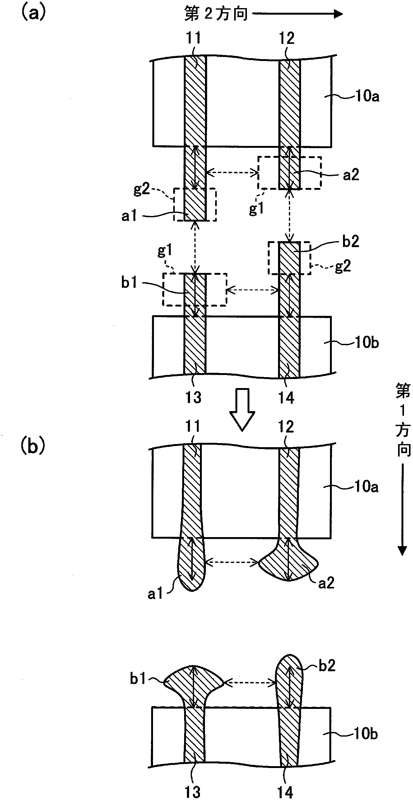
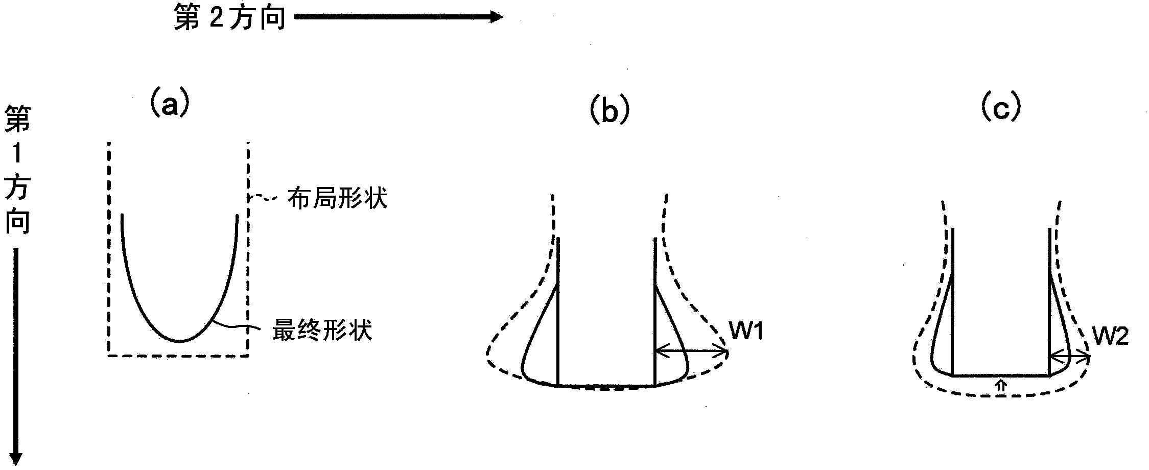
[0033] figure 1 It is a diagram showing the characteristics of the gate pattern in the semiconductor device according to the first embodiment. In this figure, (a) shows the layout shape of the gate pattern, and (b) shows the final shape of the gate pattern. in figure 1 Among them, the first and second gate patterns 11 and 12 are arranged on the active region 10a, extend in the first direction (vertical direction), and are arranged in the second direction (horizontal direction) perpendicular to the first direction . In addition, the third and fourth gate patterns 13 and 14 are arranged on the active region 10b, extend in the first direction, and are aligned in the second direction. In addition, the end portions a1 and a2 of the first and second gate patterns 11 and 12 are opposed to the opposed end portions b1 and b2 of the third and fourth gate patterns 13 and 14, respectively.
[0034] Here, it is assumed that the "gate pattern" in this embodiment is formed of polysilicon or t...
Embodiment approach 2
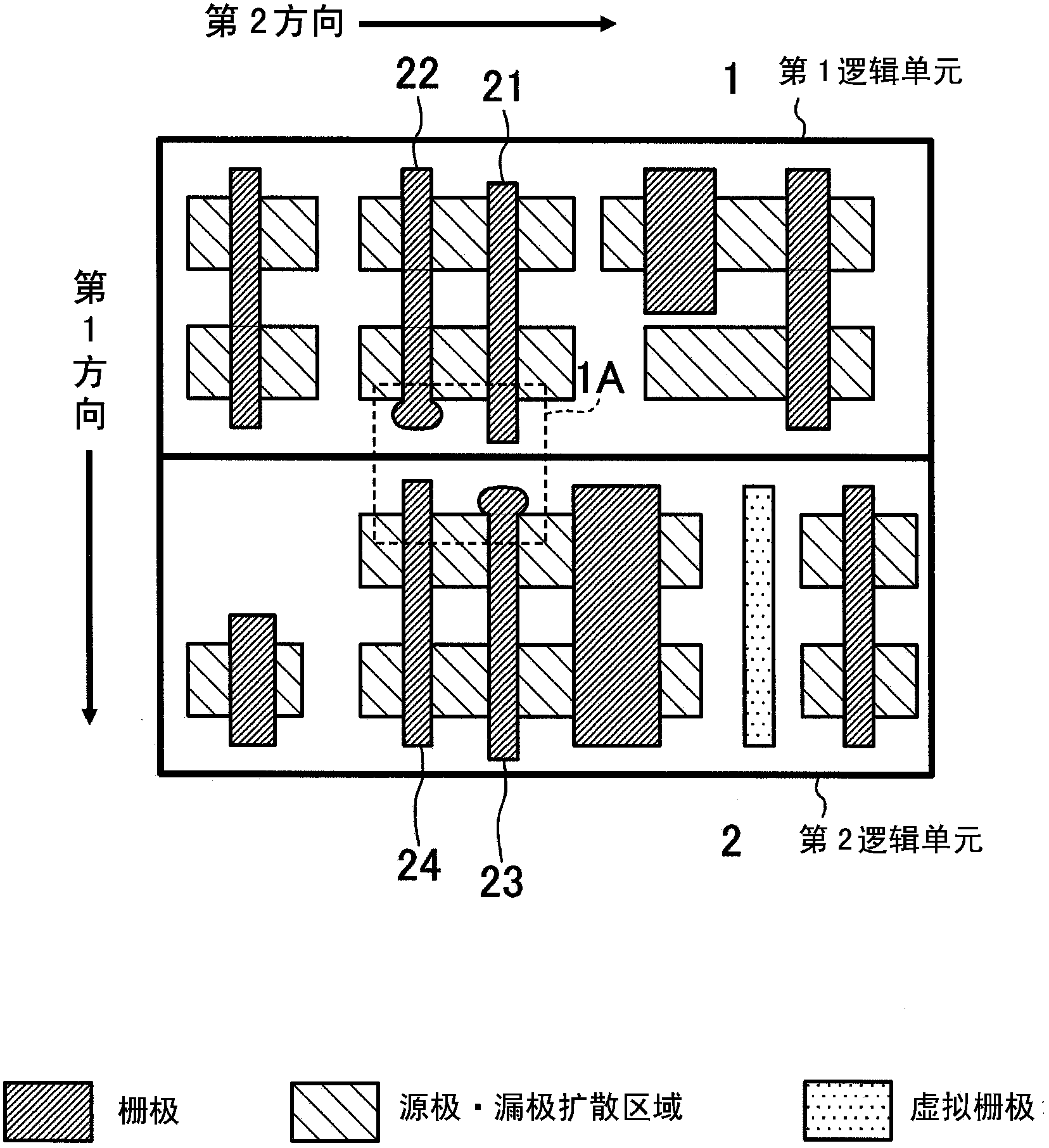
[0050] Figure 5 It is a diagram showing an example of the layout of the semiconductor device according to the second embodiment. in Figure 5 Logic units 3, 4, and 5 are arranged side by side in the longitudinal direction (first direction). The logic cells 3, 4, and 5 each have gate rows 3a, 4a, and 5a in which a plurality of gate patterns extending in the longitudinal direction are arranged in the lateral direction (the second direction orthogonal to the first direction).
[0051] The opposing end portions d1 to d10 of each gate pattern of the gate row 4a are arranged so as to face the end portions c1 to c10 of each gate pattern of the gate row 3a as the first gate row. In addition, the end portions c1, c3, c5, c7, and c9 protrude toward the logic unit 4 side compared to the end portions c2, c4, c6, c8, and c10. In addition, the opposed end portions d2, d4, d6, d8, and d10 protrude toward the logic unit 3 side compared to the opposed end portions d1, d3, d5, d7, and d9. That ...
Embodiment approach 3
[0057] Figure 7 It is a diagram for explaining the third embodiment, (a) is the circuit structure of a general 1-bit memory cell, and (b) is the layout pattern of the memory cell of (a). Figure 7 The memory cells shown in (a) and (b) include load transistors TP1 and TP2 composed of PMOS transistors, drive transistors TN1 and TN2 composed of NMOS transistors, and access transistors TN3 and TN4 composed of NMOS transistors. The gates of the load transistor TP1 and the drive transistor TN1 are connected to each other to form a first inverter INV1. Similarly, the gates of the load transistor TP2 and the drive transistor TN2 are connected to each other to form a second inverter INV2.
[0058] The node SN1 between the transistors TN1 and TP1 is connected to the gates of the transistors TN2 and TP2, and the node SN2 between the transistors TN2 and TP2 is connected to the gates of the transistors TN1 and TP1. The drain of the access transistor TN3 is connected to the node SN1, and th...
PUM
 Abstract
Description
Claims
Application Information