Materials for electronic devices

A technology of atoms and general formulas, which is applied in the field of preparation of general formula compounds and electronic devices containing general formula compounds, and can solve the problems of undisclosed aromatic system connections, etc.

Inactive Publication Date: 2012-11-21
MERCK PATENT GMBH
View PDF82 Cites 3 Cited by
  • Summary
  • Abstract
  • Description
  • Claims
  • Application Information

AI Technical Summary

Problems solved by technology

However, there is no disclosure of linking the aromatic system to an anthracenyl group via a phenylene group as described in the present application

Method used


Image

  • Materials for electronic devices
  • Materials for electronic devices
  • Materials for electronic devices

Examples


Embodiment

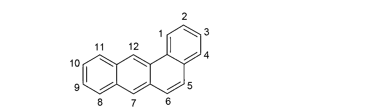
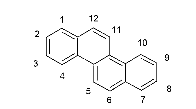
[0422] Synthesis Example 1: Preparation of 4-[3-(10-phenylanthracene-9-yl)phenyl]benzo[a]anthracene (H3)

[0423] first step:

[0424]

[0425] Use N 2 Aeration, drying of the 4 L flask by heating, first introduced 100 g (325.5 mmol) of 4-bromobenz[a]anthracene in 1400 ml of anhydrous THF. The batch was cooled to -72°C, and 190ml of 2.5M n-butyllithium was rapidly added dropwise. During this process, it was warmed from -72°C to -61°C (duration of addition: 2 minutes). The reaction mixture was stirred at -70°C for an additional 3 hours.

[0426] 150 ml (637 mmol) of triisopropyl borate were immediately injected into the solution via the dropping funnel, during which time the batch was allowed to warm to -68°C. The batch was then stirred at -70 °C for 2 h and then left to warm to room temperature. in N 2 The reaction solution was diluted with 1300 ml of ethyl acetate and 690 ml of water in a 6 L wash flask and stirred for 60 minutes. The aqueous phase is subsequently s...


PUM

PropertyMeasurementUnit
thicknessaaaaaaaaaa
thicknessaaaaaaaaaa

Abstract

The present invention relates to compounds according to the general formula (I), the use thereof in electronic devices, preferably as a host material for fluorescent dopants or as a fluorescent dopant, to methods for producing the compounds according to formula (I), and to electronic devices containing compounds according to formula (I).

Description

technical field [0001] The present invention relates to compounds of general formula (I), their use in electronic devices, methods for preparing compounds of general formula (I), and electronic devices comprising compounds of general formula (I). Background technique [0002] Organic semiconductors are being developed for many different electronic applications. The structure of organic electroluminescent devices (OLEDs) in which these organic semiconductors are used as functional materials is described, for example, in US4539507, US5151629, EP0676461 and WO98 / 27136. However, further improvements are still desired to enable these devices to be used in high quality and long life displays. Thus, in particular, the lifetime and the efficiency of blue-emitting organic electroluminescent devices currently represent problems still to be improved. Furthermore, it is necessary that the compound has high thermal stability and a high glass transition temperature and can sublimate wit...

Claims


Application Information

Patent Timeline
Patent Type & Authority Applications(China)
IPC IPC(8): C07C15/38C07C211/54C07D239/26C09K11/06H01L51/50
CPCC09K2211/1011H01L51/5012C07D471/04C07D403/12C09B3/02C07D271/10C07D403/14C07D401/10C07C2103/48C07C2103/52C07D401/14C07C2103/24C07D413/04C09B1/00C09K11/06C07D403/10C07D239/26H01L51/0071C09K2211/1014C09K2211/1044C07D333/54C07F9/5325H01L51/006C07D251/24C07F9/587C07C15/20C07D213/06C07C211/54C07D401/12C07C15/38H01L51/0067H05B33/14C09B57/001H01L51/0054C07D487/04C07C2103/42C07D241/42Y02E10/549H01L51/0058C07C2603/24C07C2603/42C07C2603/48C07C2603/52C07F9/58H10K85/622H10K85/626H10K85/633H10K85/654H10K85/657H10K50/11
Inventor 胡贝特·施普赖策约亨·施魏格尔海因里希·贝克尔弗兰克·福格斯霍尔格·海尔
Owner MERCK PATENT GMBH
Why Eureka
Try Eureka