

Compositions and methods for growing copper nanowires
A copper nanowire and copper nanotechnology, applied in the fields of nanotechnology, nanotechnology, nanostructure manufacturing, etc., can solve the problems of inefficient processing, high cost, and carbon nanotube films are not comparable to ITO.
- Summary
- Abstract
- Description
- Claims
- Application Information
AI Technical Summary
Problems solved by technology
Method used
Image

Examples
Embodiment 1
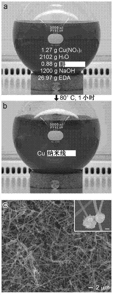
[0066] Cu(NO 3 ) 2 Copper nanowires were synthesized by reduction. For scale-up responses ( figure 1 ), 2000mL 15M NaOH, 100mL 0.2M Cu(NO 3 ) 2 , 30 mL EDA, and 2.5 mL 35 wt% hydrazine were added to the reaction flask and the reactants were mixed by hand swirling for 20 seconds after each addition. The solution was heated at 80°C and stirred at 200 rpm for 60 minutes. After 20 minutes, the solution changes from indicating Cu 2+ Ionic Royal Blue ( figure 1 A) Turns to a reddish-brown color indicating CuNW formation ( figure 1B). This reaction yielded 1.2 g of CuNWs. After the reaction, the CuNWs were washed with a 3 wt% aqueous solution of hydrazine and stored in the same hydrazine solution at room temperature under an argon atmosphere to minimize oxidation.
[0067] figure 1 C shows the scanning electron microscope (SEM, FEI XL30) image of the reaction product, which is composed of CuNWs with a diameter of 90 ± 10 nm. The inset shows a close-up of the wire showing ...
Embodiment 2
[0076] Method - General Approach: This disclosure describing specific procedures provides a method for producing long, well-dispersed copper nanowires. A major problem with existing methods of synthesizing copper nanowires is that newly formed nanowires aggregate and adhere to each other, resulting in the formation of clumps. When these agglomerates are incorporated into films, it results in poor clarity. described herein and Figure 7 The method generally shown in addresses this issue by separating the seed nucleation and wire growth processes into two steps. While not wishing to be bound by theory, it is believed that by adding surfactant immediately after nucleation of the seeds, aggregation of the nanowires is prevented during the growth phase.
[0077] In one embodiment, the scaled-up reaction yielded about 60 mg of CuNWs (percent conversion = 93%). Clean the 1000 mL round bottom flask with nitric acid and rinse it several times to ensure it is clean. The flask was th...
Embodiment 3
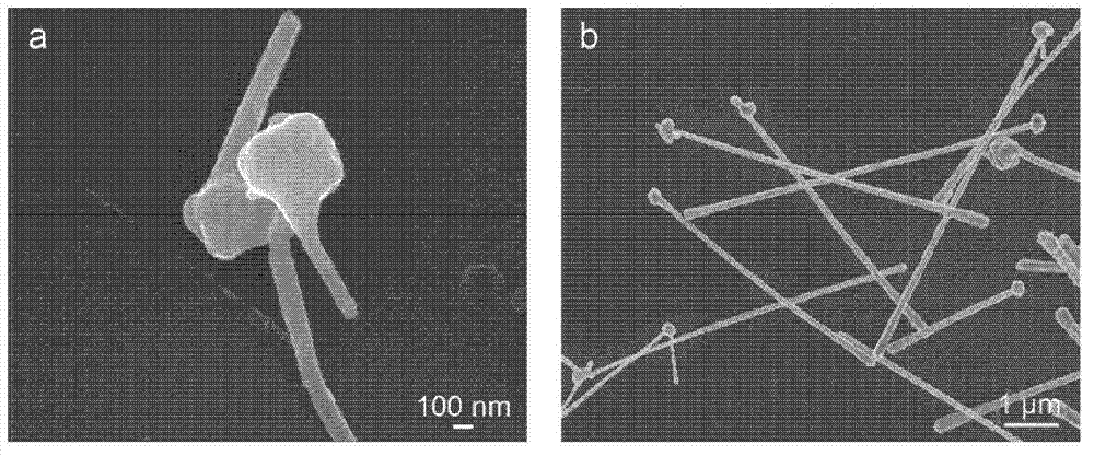
[0100] developed another synthesis that resulted in CuNWs with a diameter of about 50 nm and many nanowires with a length of more than 20 μm.
[0101] Clean the flask and stir bar with concentrated nitric acid, rinse well with DI water, and dry in an 80 °C oven before use. Once dry, the flask was allowed to cool to room temperature before adding any reactants.
[0102] By adding NaOH (20mL, 15M), Cu(NO 3 ) 2 (1 mL, 0.1 M), EDA (0.15 mL) and hydrazine (0.025 mL, 35% by weight) were added to a 50 mL round bottom flask to synthesize CuNWs. The solutions were swirled by hand for 5 seconds after each addition to mix the reactants. The solution was then heated at 80°C and stirred at 200 rpm for about 3 minutes. After the reaction, the solution was poured into a 50 mL centrifuge tube, and PVP and an aqueous solution (20 mg PVP in 5 mL of water) were gently added on top of it. The reaction solution and the PVP solution were mixed, and then placed in an ice bath. The solution was...
PUM
| Property | Measurement | Unit |
|---|---|---|
| Block resistance | aaaaa | aaaaa |
| Sheet resistance | aaaaa | aaaaa |
| Width | aaaaa | aaaaa |
Abstract
Description
Claims
Application Information