Zinc oxide (ZnO)-transistor-coupled logic (TCL) semiconductor luminescent device and method for manufacturing same
A light-emitting device and semiconductor technology, which is applied in the direction of semiconductor devices, electrical components, circuits, etc., to achieve the effects of ensuring integrity, suppressing lateral corrosion, and stable and reliable devices
- Summary
- Abstract
- Description
- Claims
- Application Information
AI Technical Summary
Problems solved by technology
Method used
Image
Examples
Embodiment 1
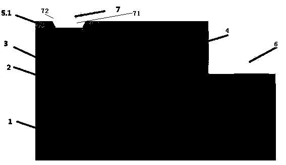
[0026] like figure 1 As shown, a semiconductor light-emitting device, which includes: a substrate 1 and a semiconductor epitaxial stack grown on the substrate, the semiconductor epitaxial stack includes: N-type layer 2, MQWS layer 3, P type layer 4 and ZnO-TCL layer 5; after etching, an N-type metal electrode 6 is evaporated on the upper surface of the N-type layer 2; a P-type metal electrode 7 is evaporated on the ZnO-TCL layer 5, and the P-type metal electrode The electrode 7 includes an embedded portion 71 embedded into the ZnO-TCL layer, and the embedded portion 71 has an embedded depth smaller than the height of the ZnO-TCL layer.
[0027] The cross section of the embedded part of the P-type metal electrode 7 is trapezoidal or bowl-shaped.
[0028] The P-type metal electrode 7 includes a protruding portion 72 placed on the upper surface of the embedded portion 71 , and the protruding portion 72 protrudes from the upper surface of the ZnO—TCL layer.
[0029] The ZnO-TCL...
Embodiment 2
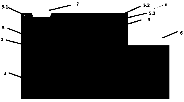
[0045] Present embodiment is except following feature, and other is all identical with embodiment 1: as figure 2 As shown, in order to reduce the operating voltage of the device more effectively, its ZnO-TCL layer 5 adopts a stacked structure ZnO:Al5.2 / ZnO:Ga5.1 / ZnO:Al5.2; and defines the P-type metal electrode 7 area When patterning, use a certain proportion of glacial acetic acid and water to perform wet etching to etch the ZnO-TCL layer 5 to the ZnO:Ga layer 5.1.
Embodiment 3
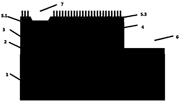
[0047] Present embodiment is except following feature, and other is all identical with embodiment 1: as image 3 As shown, in order to reduce the operating voltage of the device more effectively and improve the light extraction efficiency of the device in this embodiment, the ZnO-TCL layer 5 adopts a stacked structure ZnO: Ga5.1 / ZnO5.3, and the growth process is changed by changing the growth Process parameters, so that the ZnO layer 5.3 presents a nanowire structure; when defining the region and pattern of the P-type metal electrode 7, use a certain proportion of glacial acetic acid and water to perform wet etching to etch the ZnO-TCL layer 5 to the ZnO:Ga layer 5.1 .
PUM
 Abstract
Description
Claims
Application Information


