
Light amplifier and laser processing device

A technology of optical amplification and excitation light, which can be used in lasers, laser welding equipment, laser parts, etc., and can solve problems such as detection of peaks

Active Publication Date: 2012-11-28
OMRON CORP
View PDF5 Cites 1 Cited by
  • Summary
  • Abstract
  • Description
  • Claims
  • Application Information

AI Technical Summary

Problems solved by technology

Therefore, in the case of fiber amplifiers, it is more difficult to detect the peak for each pulse

Method used


Image

  • Light amplifier and laser processing device
  • Light amplifier and laser processing device
  • Light amplifier and laser processing device

Examples


no. 1 approach >

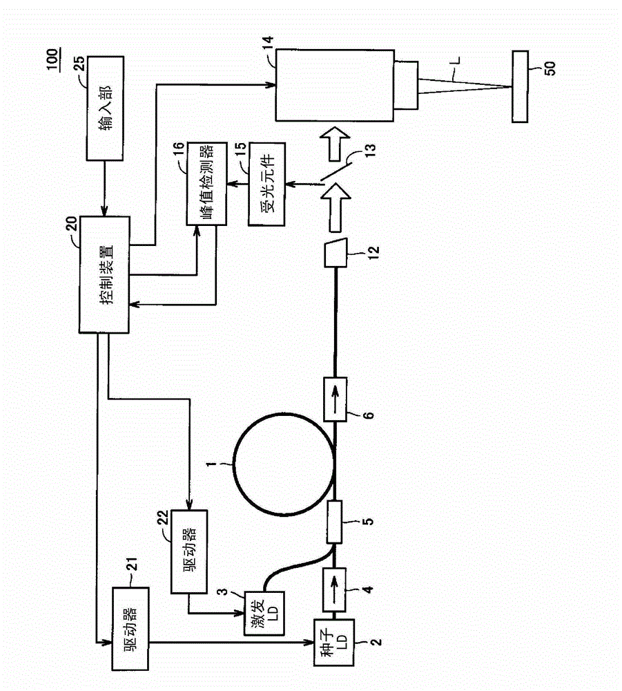
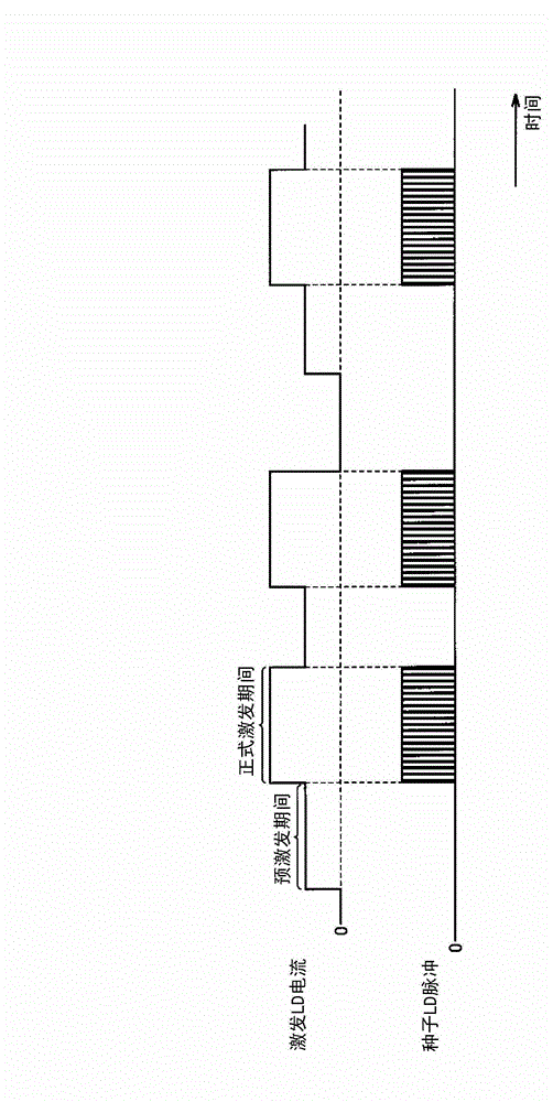
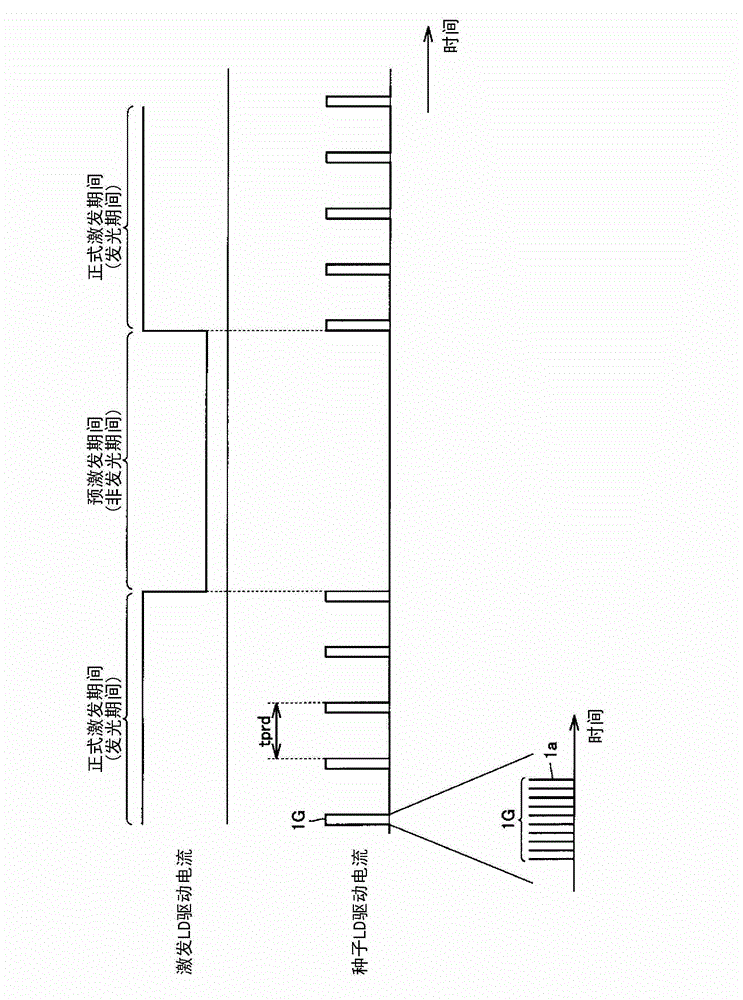
[0063] figure 1 It is a figure which shows the structural example of the laser processing apparatus which concerns on 1st Embodiment of this invention. refer to figure 1, the laser processing device 100 includes an optical amplifying device and a laser beam scanning mechanism 14, wherein the laser beam scanning mechanism 14 is used for scanning with laser light from the optical amplifying device. The optical amplification device has: optical amplification fiber 1; seed LD2; excitation LD3; isolator 4, 6; synthesizer 5; end cap 12; driver 21, 22; ; Input unit 25 .

[0064] The optical amplifying fiber 1 has: a core, which is an optical amplifying component, and rare earth elements are added to the core; and a metal clad (clad), which is provided around the core. The types of rare earth elements added to the fiber core are not particularly limited, and examples include Er (erbium), Yb (ytterbium), and Nd (neodymium). The case where the rare earth element is Yb will be descri...

no. 2 approach >

[0113] Figure 13 It is a block diagram of the laser processing apparatus of 2nd Embodiment. refer to Figure 13 , the laser processing device 101 has an optical amplifier composed of two-stage optical fiber amplifiers. The laser processing apparatus of the second embodiment differs from the laser processing apparatus of the first embodiment in this point. refer to figure 1 and Figure 13 , The difference between the laser processing device 101 and the laser processing device 100 is that the laser processing device 101 also has: a coupler 7; an optical amplification fiber 8; an excitation LD9A, 9B; a synthesizer 10; device 18; driver 23.

[0114] The coupler 7 divides the optical pulse output from the optical amplifying fiber 1 via the isolator 6 into an optical pulse to be sent to the combiner 10 and an optical pulse to be sent to the light receiving element 17 . The combiner 10 combines the laser light from the coupler 7 and the laser light from the excitation LDs 9A and...


PUM


Abstract

A light amplifier and a laser processing device are provided. A peak value detector (16) detects power of an output light pulse which is output from the light amplifying fiber. A light receiving element (15) receives a group of light pulses including a plurality of pulses and converts the group of light pulses into a current signal. A current / voltage converter circuit (31) converts the current output from the light receiving element (15) to voltage. An integration circuit (32) integrates the voltage output from the current / voltage converter circuit (31). A programmable gain amplifier (PGA) (33) amplifies the signal output from the integration circuit (32) and provides the signal for an A / D converter circuit (34). The gain of the PGA (33) is set by a gain setting signal from a signal processing circuit (40). The signal processing circuit (40) adjusts the gain of the PGA (33) so that the gain increases as the repetition frequency of the group of pulses increases.

Description

technical field [0001] The present invention relates to an optical amplifier and a laser processing device, and more particularly to a technique for stably generating optical pulses from an optical fiber amplifier of the MOPA (Master Oscillator and Power Amplifier) ​​system. Background technique [0002] In a laser processing device, the power of the laser affects the processing quality. Therefore, techniques for controlling the power of laser light emitted from laser processing apparatuses have been proposed so far. [0003] For example, Japanese Patent Application Laid-Open No. 2010-10274 (Patent Document 1) discloses a structure in which the average power and peak power of a laser pulse output from a fiber laser oscillator are measured, and the measurement results are fed back to an LD (laser diode) drive circuit. . [0004] In addition, for example, Japanese Patent Application Laid-Open No. 2010-171131 (Patent Document 2) discloses a method of emitting a laser source f...

Claims


Application Information

Patent Timeline
Patent Type & Authority Applications(China)
IPC IPC(8): H01S3/067H01S3/13B23K26/06B23K26/00H01S3/00
CPCH01S3/067H01S3/06758H01S3/10015H01S3/1312H01S3/094076H01S3/1305H01S3/06754B23K26/063H01S3/09415H01S3/094H01S3/131H01S3/1301H01S3/10069B23K26/0622H01S3/13013
Inventor 大垣龙男
Owner OMRON CORP
Features
  • Generate Ideas
  • Intellectual Property
  • Life Sciences
  • Materials
  • Tech Scout
  • Unparalleled Data Quality
  • Higher Quality Content
  • 60% Fewer Hallucinations
Learn More