Method for arranging metal palladium layer in conducting layer of printed circuit board and layered structure thereof

A technology for printed circuit boards and conductive layers, applied in printed circuits, printed circuit manufacturing, printed circuit components, etc., can solve the problems of brittle electroplating, high cost, shortened service life, etc., to reduce thickness and reduce material costs Effect

Active Publication Date: 2012-11-28
深圳和美精艺半导体科技股份有限公司
View PDF5 Cites 22 Cited by
  • Summary
  • Abstract
  • Description
  • Claims
  • Application Information

AI Technical Summary

Problems solved by technology

Soldering normally causes embrittlement of the electroplated gold which will shorten service life so avoid soldering over electroless gold, while electroless nickel/immersion gold embrittlement rarely occurs due to thin and consistent gold
[0005] However, in the current market for packaging printed circuit boards, as the position of soft gold solder joints, the thickness of the gold

Method used


Image

  • Method for arranging metal palladium layer in conducting layer of printed circuit board and layered structure thereof
  • Method for arranging metal palladium layer in conducting layer of printed circuit board and layered structure thereof
  • Method for arranging metal palladium layer in conducting layer of printed circuit board and layered structure thereof

Examples


Embodiment Construction

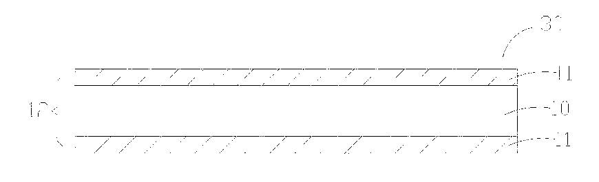
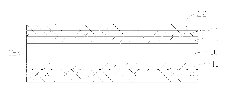
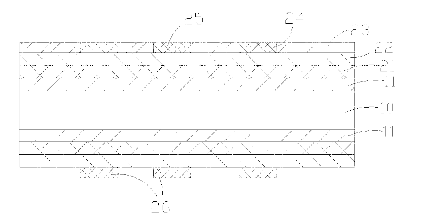
[0042] Such as Figures 1 to 6 Shown, a kind of method that metal palladium layer is set in the conductive layer of printed circuit board, it is characterized in that, comprises the steps:

[0043] In the first step, copper cladding is performed on the insulating substrate 10 , and copper foil 11 is coated on one side or both sides of the insulating substrate 10 to form a copper clad laminate 12 .

[0044] Specifically, it may be determined according to production requirements whether to coat copper on one side or both sides of the insulating substrate 10 .

[0045] In the present invention, if adopt the mode of electroplating to carry out copper cladding, due to double-sided simultaneous electroplating during electroplating, when requiring layer to thicken copper plating, also can be thickened copper plating on another layer, if copper plating is too thick, will It affects the subsequent circuit fabrication, so it is necessary to thin the copper plating layer, so the acidic ...


PUM

PropertyMeasurementUnit
Thicknessaaaaaaaaaa
Thicknessaaaaaaaaaa

Abstract

The invention relates to a method for arranging a metal palladium layer in a conducting layer of a printed circuit board and a layered structure thereof. The method comprises the following steps of: firstly, coating copper on an insulating substrate, and baking the substrate; then, sequentially carrying out the processes of drilling, copper precipitation, line manufacturing and insulating layer solder resisting so as to obtain a half-finished product of a board body; and finally, sequentially carrying out the processes of nickel precipitation, palladium precipitation and gold precipitation to the line part of the half-finished product of the board body. In the process of plating soft gold on the printed circuit board, a metal palladium layer is arranged between a nickel layer and a gold layer, so that the thickness of the gold layer can be greatly reduced so as to achieve the effect of lowering the material cost.

Description

technical field [0001] The invention relates to a method for manufacturing a printed circuit board and its layered structure, in particular to a method for setting a metal palladium layer between a nickel layer and a gold layer in the process of soft gold plating on a printed circuit board and its layer shape structure. Background technique [0002] Printed circuit boards, also known as printed circuit boards, are devices that provide electrical connections for electronic components. The main advantage of using printed circuit boards during implementation is that they can greatly reduce wiring and assembly errors, and can improve automation levels and production labor. efficiency. The printed circuit board is based on an insulating board, cut to a certain size, with at least one conductive pattern on it, and holes, such as component holes, fastening holes, metallized holes, etc., which can be used to replace In the past, the chassis of electronic components was installed,...

Claims


Application Information

Patent Timeline
IPC IPC(8): H05K3/24H05K3/18H05K1/09
Inventor 岳长来
Owner 深圳和美精艺半导体科技股份有限公司
Why Eureka
Try Eureka