Organic electronic device and method for manufacturing the same

A technology of organic electronic devices and manufacturing methods, applied in semiconductor/solid-state device manufacturing, electrical solid-state devices, electrical components, etc., can solve problems such as weak tolerance

Active Publication Date: 2012-11-28
MITSUBISHI RAYON CO LTD
View PDF7 Cites 11 Cited by
  • Summary
  • Abstract
  • Description
  • Claims
  • Application Information

AI Technical Summary

Problems solved by technology

However, it is known that among solar cell elements, organic thin-film solar cell elements developed in recent years have weak resistance to moisture, oxygen, or organic substances generated by heat from constituent parts. Long life, these factors must be excluded as much as possible

Method used


Image

  • Organic electronic device and method for manufacturing the same
  • Organic electronic device and method for manufacturing the same
  • Organic electronic device and method for manufacturing the same

Examples


Embodiment approach 1

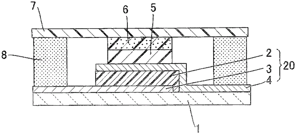
[0089] An example of the organic electronic device of the present invention is figure 1 As shown, an organic semiconductor element (B) 20, a layer (C) 6 containing a scavenger that absorbs at least one of moisture and oxygen, and a gas barrier film (D) 7 are laminated in this order. The organic semiconductor element (B) 20 has at least a pair of electrodes 3, 4 and an organic semiconductor layer 2. The gas barrier film (D) 7 covers the organic semiconductor element 20, wherein at least one of the electrodes is There is at least one anticorrosion layer (E) 5 between the layers (C) 6 of the scavenger absorbing at least one of moisture and oxygen. Among them, the organic semiconductor element (B) 20 may be formed on the substrate (A) 1, and the gas barrier film (D) may also be used as the substrate. Among them, the organic semiconductor element (B) has the following structure: the organic semiconductor layer 2 is provided between the transparent electrode 3 and the metal electrode...

Embodiment approach 2

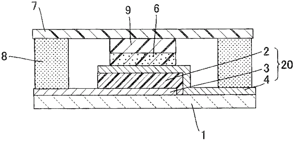
[0096] In addition, an example of the organic electronic device of the present invention is image 3 and Figure 4 As shown, at least a substrate (A) 1, an organic semiconductor element (B) 20, a layer (C) 6 containing a scavenger that absorbs moisture and / or oxygen, and a gas barrier film (D) 7 are laminated in this order, wherein , There is a resin layer (F) between the organic semiconductor element (B) and the layer (C) 6 containing a scavenger that absorbs at least one of moisture and oxygen, so that the organic semiconductor element (B) ) Is not in direct contact with the layer (C) 6, and the substrate (A) 1 and the gas barrier film (D) 7 are directly bonded or bonded via an intermediate layer such as an anti-corrosion layer (E) 5, So that the organic semiconductor element (B) and the layer (C) 6 are not in contact with external air,

[0097] Furthermore, the film thickness of the resin layer (F) is 20 μm or more,

[0098] The resin layer (F) and the gas barrier film (D) sati...

Embodiment approach 3

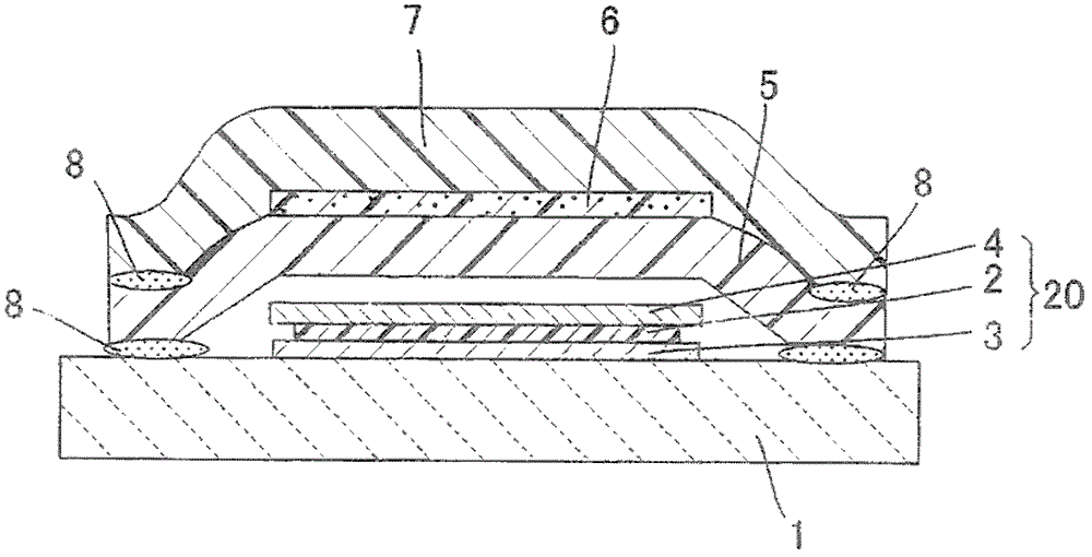
[0104] In addition, an example of the organic electronic device of the present invention is Figure 5 As shown, a layer (C) 6 containing a trapping agent is formed on a gas barrier film (D) 7 on which a gas barrier layer such as a back protective sheet not shown in the figure is formed, and a layer (C) 6 composed of a corrosion protection layer (E) 5 is provided The resin layer (F) is made to cover the capture agent-containing layer (C) 6, and the resin layer (F) is bonded to the gas barrier film (D) 7 via the sealing material 8 to make the resin layer (F ) Not in contact with the end surface of the organic electronic device and not exposed to the outside. The other parts are the same as in the second embodiment described above.


PUM


Abstract

The invention provides an organic electronic device which does not deteriorate the device performance over a long period of time, for example, a thin film organic solar cell element in which a lowering of the power generation efficiency is suppressed, and a method for manufacturing the organic electronic device. Disclosed is an organic electronic device formed by laminating an organic semiconductor element (B) provided with at least a pair of electrodes, a layer (C) containing a scavenger which absorbs at least one of water and oxygen, and a gas barrier film (d) in this order, wherein one or plural anticorrosion layers (E) is provided between at least one of the pair of electrodes and the layer (C) containing a scavenger which absorbs at least one of water and oxygen; the thickness of the anticorrosion layer (E) is 20 [mu]m or more; the moisture vapor transmission rate (Pe) (g / m2 / day) of the anticorrosion layer (E) in 40 DEG C and 90% RH environment with respect to the moisture vapor transmission rate (Pd) of the gas barrier film (D) in 40 DEG C and 90%RH environment satisfies a condition of 15 g / m2 / day>=Pe>Pd; and the moisture vapor transmission rate (Pd) of the gas barrier film (D) satisfies a condition of 10<->4<=Pd<=10<-1> g / m2 / day.

Description

Technical field [0001] The invention relates to an organic electronic device and a manufacturing method of the organic electronic device. Background technique [0002] In the past, as a technology for protecting solar cells, in order to achieve weight reduction and thinning, a technology for covering solar cells with a film has been proposed. Generally, solar cell modules are formed using, for example, crystalline silicon solar cell elements or amorphous silicon solar cell elements. Using such solar cell elements, the solar cell module is manufactured by a lamination method, etc., in accordance with, for example, a surface protective sheet layer, a filler layer, a solar cell element as a photovoltaic element, a filler layer, and The back surface protective sheet layer is laminated in order, and then vacuum suction is performed, followed by heating and pressure bonding. However, it is known that among solar cell elements, organic thin-film solar cell elements developed in recent...

Claims


Application Information

Patent Timeline
Patent Type & Authority Applications(China)
IPC IPC(8): H01L51/42
CPCH01L51/42H01L51/448Y02E10/50H01L51/5259H01L51/5253Y02E10/549Y02P70/50H10K30/00H10K30/88H10K50/846H10K50/844
Inventor 大泉淳一船山胜矢藤原崇志米山孝裕半田敬信
Owner MITSUBISHI RAYON CO LTD
Why Eureka
Try Eureka