Silicon-based near-infrared quantum-dot electroluminescent device and preparation method thereof

A near-infrared and quantum dot technology, applied in electrical components, semiconductor devices, circuits, etc., can solve problems such as low luminous efficiency

Inactive Publication Date: 2012-12-12
INST OF SEMICONDUCTORS - CHINESE ACAD OF SCI
View PDF4 Cites 4 Cited by
  • Summary
  • Abstract
  • Description
  • Claims
  • Application Information

AI Technical Summary

Problems solved by technology

[0002] Silicon (Si) is an important semiconductor integrated circuit material, but because silicon is an indirect bandgap material, the luminous effici...

Method used


Image

  • Silicon-based near-infrared quantum-dot electroluminescent device and preparation method thereof
  • Silicon-based near-infrared quantum-dot electroluminescent device and preparation method thereof

Examples


Embodiment Construction

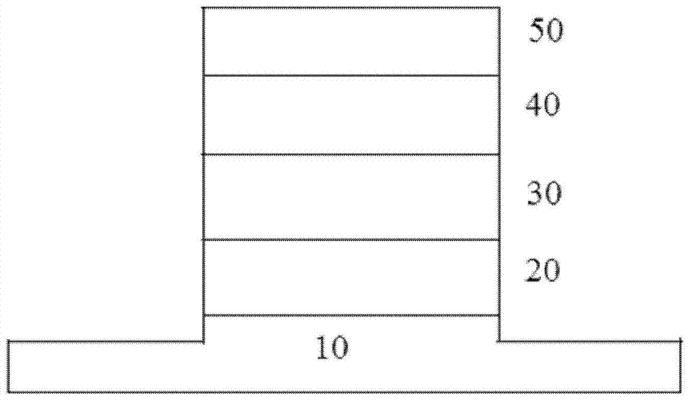
[0022] see figure 1 and figure 2 As shown, the present invention provides a near-infrared quantum dot electroluminescent device on a silicon base, comprising:

[0023] A substrate 10, the material of the substrate 10 is a heavily doped p-type or n-type complete silicon material, or a heavily doped p-type or n-type SOI material, and the resistivity of the heavily doped silicon or SOI is less than 25Ω cm, the substrate 10 is used as an electrode to inject holes into the device;

[0024] An oxide layer 20, the oxide layer 20 is made on the substrate 10 by rapid thermal oxidation or high temperature and low pressure oxidation, the oxide layer 20 is a silicon dioxide film with a thickness of 1-5nm, which changes the substrate by sharing the voltage The Fermi level of silicon and the position of the conduction band and valence band energy level of the light-emitting layer are used to balance the injection of electrons and holes, thereby increasing the probability of radiative rec...


PUM

PropertyMeasurementUnit
Resistivityaaaaaaaaaa
Thicknessaaaaaaaaaa
Luminous wavelengthaaaaaaaaaa

Abstract

A silicon-based near-infrared quantum-dot electroluminescent device comprises a substrate, an oxidation layer, a light-emitting layer, an electron transporting layer and a metal electrode, wherein the oxidation layer which is a silicon dioxide film is prepared on the substrate and is used for balancing electron and hole injection by means of voltage sharing; the light-emitting layer is prepared on the oxidation layer and is composed of near-infrared light-emitting colloidal quantum dots; the electron transporting layer is prepared on the light-emitting layer and can transport electrons and improve carrier injection efficiency; and the metal electrode is prepared on the electron transporting layer and used for injecting electrons into the light-emitting layer. Each of the substrate, the oxidation layer, the light-emitting layer, the electron transporting layer and the metal electrode is of a planar waveguide structure or a ridge waveguide structure, the substrate of the ridge waveguide structure is convex, a boss is arranged in the middle of the substrate, and the oxidation layer, the light-emitting layer, the electron transporting layer and the metal electrode are all prepared on the boss of the substrate. The silicon-based near-infrared quantum-dot electroluminescent device is tunable in light-emitting frequency, and the preparation method is available to materials, low in production cost and simple in process.

Description

technical field [0001] The invention relates to an electroluminescence device, in particular to a near-infrared quantum dot electroluminescence device on a silicon base and a preparation method thereof. Background technique [0002] Silicon (Si) is an important semiconductor integrated circuit material, but because silicon is an indirect bandgap material, the luminous efficiency is low. Research work on materials and devices, such as integrating III-V light-emitting materials on silicon substrates, or making porous silicon, etc. Silicon-based near-infrared light source is expected to be used in optical communication, combined with mature CMOS technology, as a light source for optoelectronic integration or even all-optical communication. [0003] Colloidal quantum dots are a new type of quantum dot material, which are crystal particles with a particle size of nanometer scale, which can be synthesized by chemical methods. Therefore, unlike the quantum dots obtained by tradit...

Claims


Application Information

Patent Timeline
IPC IPC(8): H01L33/06H01L33/20
Inventor 许兴胜李成果
Owner INST OF SEMICONDUCTORS - CHINESE ACAD OF SCI
Why Eureka
Try Eureka