Field programmable gate array (FPGA) prototype verification device and method

A technology for prototype verification and signal selection, applied in special data processing applications, instruments, electrical digital data processing, etc., can solve the problems of short signal length, time-consuming more than ten to twenty hours, low positioning error efficiency, etc. Improve operability, increase signal types, and save time

Active Publication Date: 2013-01-02
SPREADTRUM COMM (SHANGHAI) CO LTD
View PDF2 Cites 9 Cited by
  • Summary
  • Abstract
  • Description
  • Claims
  • Application Information

AI Technical Summary

Problems solved by technology

For large-scale SoC FPGA prototype verification, it will take more than ten to twenty hours to change the pin constraint each time, which has poor operability and low efficiency.
[0013] 2) Using an oscilloscope to observe the signals inside the FPGA in real time will face the shortcomings of too few observable signals and too short signal length, and the visibility is poor, so the efficiency of positioning errors is relatively low
[0021] 1) Because the problem of locating the FPGA operation error is mainly adopted the method of elimination, it is first judged that the position most relevant to the current error is a problem, and then it is normal to exclude these positions one by one according to the degree of correlation, so the prior art 2 will be repea

Method used


Image

  • Field programmable gate array (FPGA) prototype verification device and method
  • Field programmable gate array (FPGA) prototype verification device and method
  • Field programmable gate array (FPGA) prototype verification device and method

Examples


Embodiment Construction

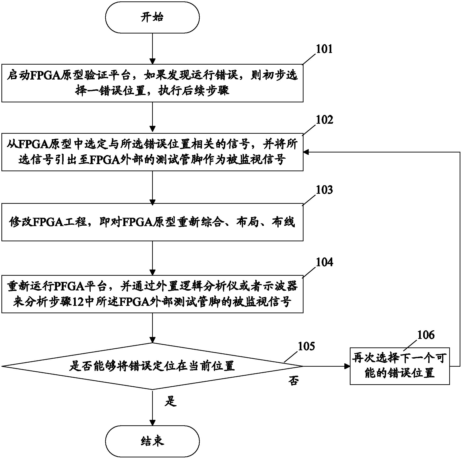
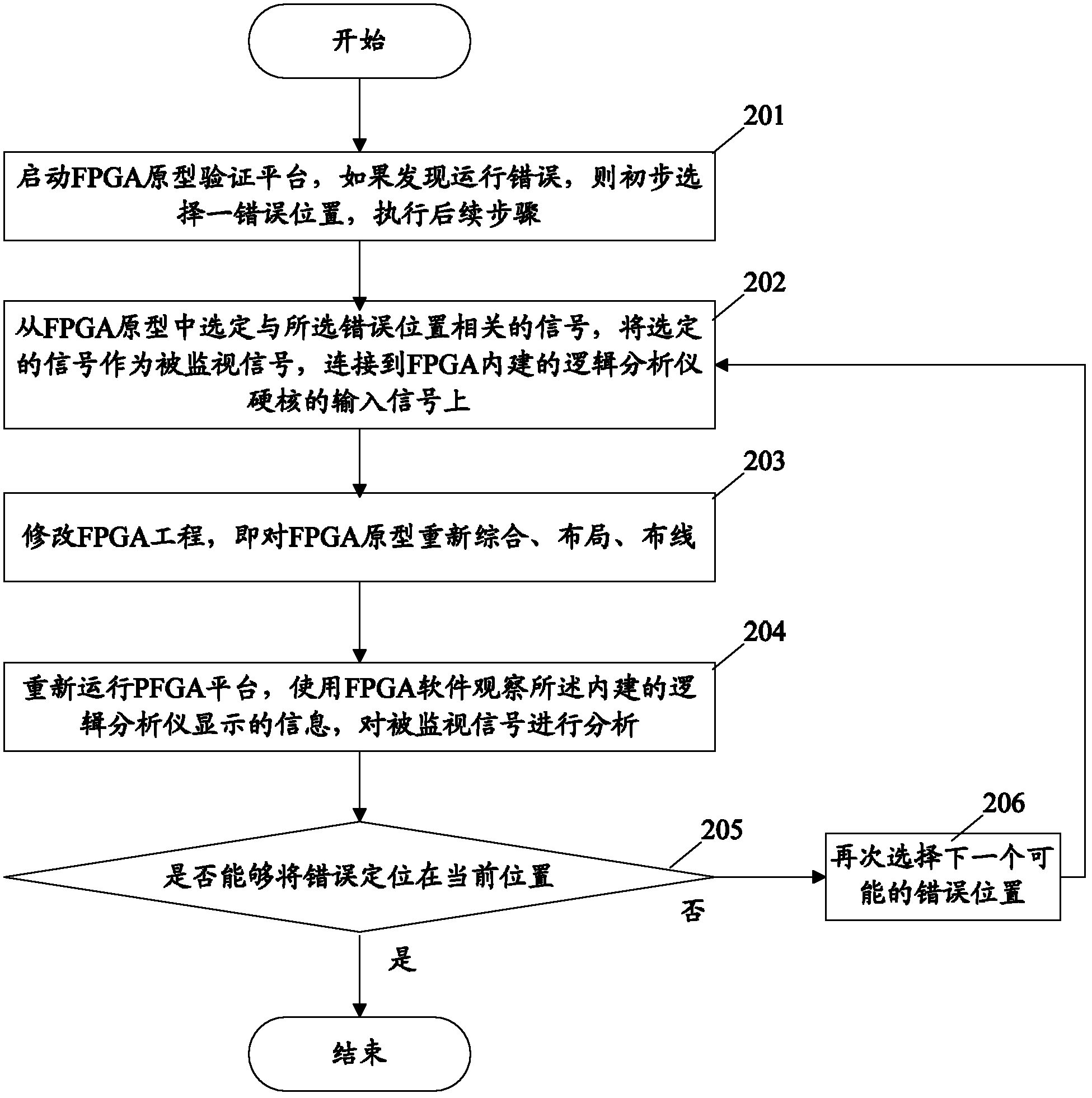
[0062] The present invention will be further described in detail below in conjunction with the accompanying drawings and specific embodiments.

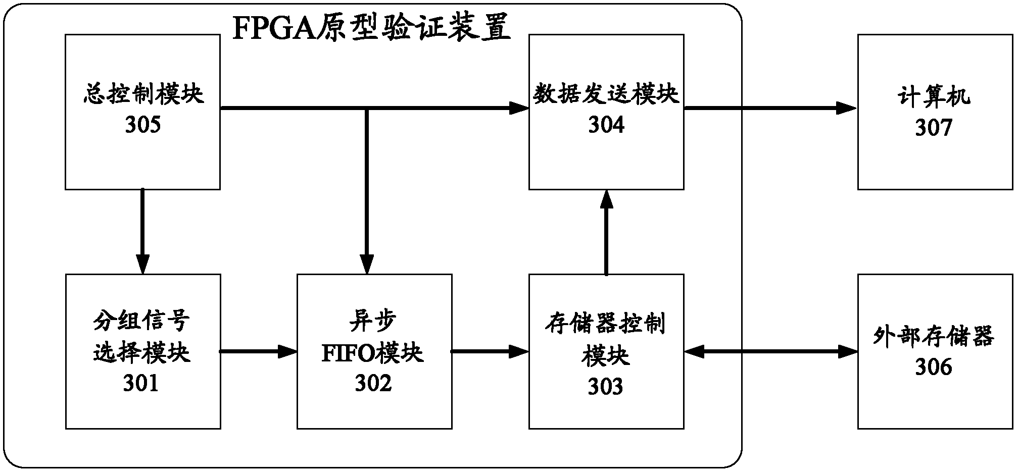
[0063] image 3 It is a structural block diagram of an embodiment of the FPGA prototype verification device of the present invention. see image 3 , the device includes: a packet signal selection module 301 , an asynchronous FIFO module 302 , a memory control module 303 , a data sending module 304 and a general control module 305 .

[0064] The grouping signal selection module 301 has more than one input terminal and one output terminal, and its input terminal is connected to at least one group of grouping signals of the FPGA prototype, and one group of grouping signals is input to one input terminal in parallel, and the grouping signal selection module 301 selects according to the selected The instruction selects one of the grouped signals at its input as a monitored signal and outputs the monitored signal at its output.

[0065] ...


PUM


Abstract

The invention discloses field programmable gate array (FPGA) prototype verification device and method. The device comprises a packet signal selection module, an asynchronous first in first out (FIFO) module, a memory control module, a data transmission module and a main control module, wherein an input end of the packet signal selection module is connected with at least one packet signal of an FPGA prototype; when an error occurs during the FPGA prototype verification, one of the packet signals is selected from the input end of the packet signal selection module according to a selection instruction to serve as a monitored signal; the packet signal is output to the asynchronous FIFO module to be synchronized into a signal with a speed same as that of the memory control module; the synchronized signal is stored to an external memory by the memory control module and then is read to the data transmission module by the external memory; and the monitored signal is transmitted to an external computer by the data transmission module to carry out data analysis so as to positioning the error. By using the FPGA prototype verification device and method, the operability, the visibility and the efficiency of the FPGA verification can be improved.

Description

technical field [0001] The invention relates to a field programmable gate array (FPGA, Field Programmable Gate Array) prototype verification technology, in particular to an FPGA prototype verification device and a verification method. Background technique [0002] System prototype verification is a key factor for the success of system on chip (SoC, System on Chip) and application specific integrated circuit (ASIC, Application Specific Integrated Circuit) design. Traditional verification methods include software simulation technology and hardware accelerator technology. The software simulation technology uses software to simulate SoC or ASIC design and verify it. Its advantage is that it has absolute visibility for the design, and its disadvantage is that the simulation speed is slow. As SoC designs become more and more complex, designers find it difficult to verify the correctness of hardware design only by software simulation due to the limitation of simulation speed and m...

Claims


Application Information

Patent Timeline
IPC IPC(8): G06F17/50
Inventor 高峰王明耀
Owner SPREADTRUM COMM (SHANGHAI) CO LTD
Why Eureka
Try Eureka