Method for manufacturing shallow trench isolation

A manufacturing method and shallow trench technology, which are applied in semiconductor/solid-state device manufacturing, electrical components, circuits, etc., can solve problems such as device performance degradation and STI sidewall roughness, and achieve the effect of reducing roughness.

Inactive Publication Date: 2013-01-09
SEMICON MFG INT (SHANGHAI) CORP
View PDF1 Cites 13 Cited by
  • Summary
  • Abstract
  • Description
  • Claims
  • Application Information

AI Technical Summary

Problems solved by technology

[0006] The invention provides a method for manufacturing shallow trench isolation, which solves the problem of device performance degradation caused by rough side walls of existing STIs

Method used


Image

  • Method for manufacturing shallow trench isolation
  • Method for manufacturing shallow trench isolation
  • Method for manufacturing shallow trench isolation

Examples


Embodiment Construction

[0021] The principles and features of the present invention are described below in conjunction with the accompanying drawings, and the examples given are only used to explain the present invention, and are not intended to limit the scope of the present invention.

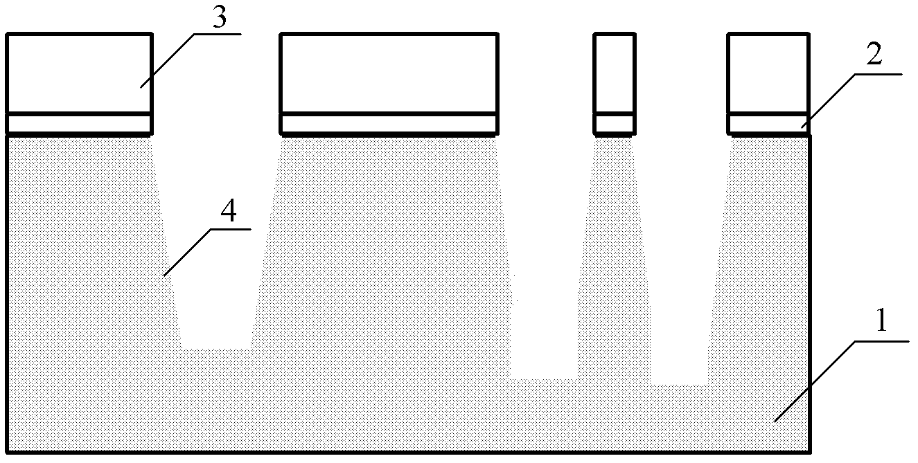
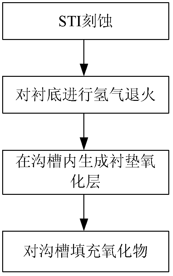
[0022] In the present invention, in order to solve the problems in the prior art, in the process of manufacturing the STI structure, the substrate is subjected to hydrogen annealing treatment after the shallow trenches are formed by etching, so that the rough shallow trench side walls become smooth and shallow. The corners at the bottom of the trench are also rounded, thereby improving the performance of semiconductor devices and integrated circuits.

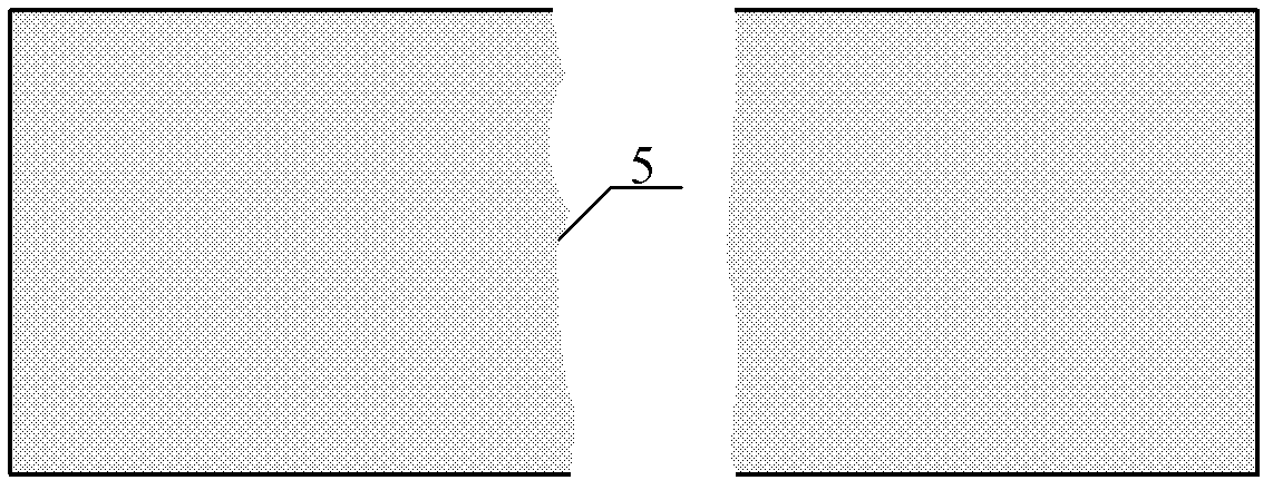
[0023] Such as figure 2 and combine Figure 3a and Figure 3b As shown, as an embodiment of the present invention, when forming shallow trench isolation on the Si substrate 21, a pad oxide layer 22 is first formed on the Si substrate, and a pad oxide layer 22 is de...


PUM


Abstract

The invention provides a method for manufacturing shallow trench isolation. After being etched to form a shallow trench, a substrate is subject to an annealing process under a certain condition of hydrogen atmosphere, so that element atoms of the substrate are promoted to make thermal motion migration under a high temperature, side walls of the rough shallow trench and square corners of the shallow trench become smooth, the leakage current of a semiconductor device employing the shallow trench isolation is reduced, and the performances of the semiconductor device and an integrated circuit are improved.

Description

technical field [0001] The invention relates to the manufacturing technology of semiconductor devices, in particular to a manufacturing method of shallow trench isolation. Background technique [0002] As the microelectronics process enters the deep submicron stage, in order to realize high-density, high-performance large-scale integrated circuits, the isolation process between semiconductor devices becomes more and more important. The prior art generally uses Shallow Trench Isolation (STI, Shallow Trench Isolation) to realize the isolation of active devices, such as in CMOS (Complementary Metal Oxide Semiconductor, Complementary Metal Oxide Semiconductor) devices, NMOS (N-Mental-Oxide- The isolation layer between the Semiconductor (N-type metal oxide semiconductor) transistor and the PMOS (P-Mental-Oxide-Semiconductor, P-type metal oxide semiconductor) transistor is formed by the STI process. [0003] Such as Figure 1a As shown, the existing STI process flow is usually on...

Claims


Application Information

Patent Timeline
Patent Type & Authority Applications(China)
IPC IPC(8): H01L21/762
Inventor 王冬江胡敏达张海洋
Owner SEMICON MFG INT (SHANGHAI) CORP
Why Eureka
Try Eureka