Manufacturing method of single plating hole copper

A production method and hole copper technology, applied in the direction of electrical connection formation of printing components, etc., can solve the problems of uneven copper plating, low production efficiency, and the inability of electroplating copper to meet requirements.

Active Publication Date: 2013-01-16
JIANGNAN INST OF COMPUTING TECH
View PDF1 Cites 27 Cited by
  • Summary
  • Abstract
  • Description
  • Claims
  • Application Information

AI Technical Summary

Problems solved by technology

[0004] However, in the PCB copper plating process, due to the influence of current distribution on the board surface, there will be certain differences in the thickness of copper plated in different areas of the printed circuit board. For printed circuit boards that require strict copper uniformity on the opposite side, conventional copper plating cannot meet needs
[0005] Moreover, due to the influence of current distribution factors on the surface of the printed circuit board during the copper electroplating process, there are certain differences in the thickness of copper electroplated in different areas of the printed circuit board, which will affect the subsequent process of the printed circuit board and the electrical characteristics of the printed circuit board. The performance is greatly affected, and even the printed circuit board will be scrapped in severe cases
[0006] To solve the problem of uneven copper plating, it is possible to increase the size of the printed circuit board, use low-current long-term electroplating and turn-around electroplating, but this cannot fundamentally solve the problem of uneven copper plating in the electroplating process, and the production efficiency is low
For printed circuit boards with extremely high requirements on the uniformity of copper thickness on the board surface, conventional production methods can no longer meet the production requirements

Method used


Image

  • Manufacturing method of single plating hole copper
  • Manufacturing method of single plating hole copper
  • Manufacturing method of single plating hole copper

Examples


Embodiment Construction

[0026] In order to make the content of the present invention clearer and easier to understand, the content of the present invention will be described in detail below in conjunction with specific embodiments and accompanying drawings.

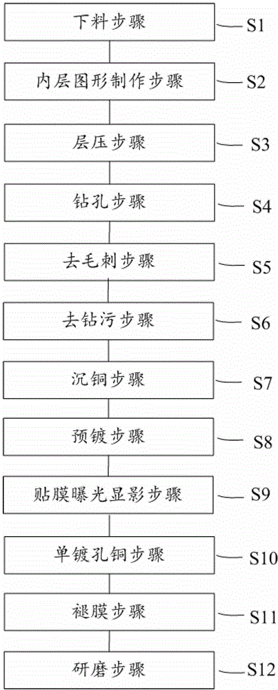
[0027] figure 1 A flow chart of a method for manufacturing single-plated-hole copper according to an embodiment of the present invention is schematically shown. Among them, single-plated copper is an electroplating process that protects the board surface with a dry film and only electroplates copper on the hole wall.

[0028] More specifically, as figure 1 As shown, the manufacturing method of single plated hole copper according to the embodiment of the present invention comprises:

[0029] Cutting step S1: preparing the substrate as a printed circuit board, and cutting the substrate, for example, cutting the substrate into a required size;

[0030] Step S2 of making inner-layer graphics: executing each inner-layer circuit graphics of the mul...


PUM


Abstract

The invention provides a manufacturing method of single plating hole copper. The manufacturing method comprises the following steps: preparing a base plate as a printed circuit board, and cutting off the base plate; manufacturing each circuitous pattern of a multi-layer plate; laminating the inner layer circuitous pattern, an insulation material and an outer layer of copper foil together so as to form an integral printed circuit board structure; drilling holes with predetermined hole diameters on the surface of the printed circuit board; sinking a layer of copper on a hole wall, thus the original non-conductive hole wall is conductive; coating a layer of pre-plated copper on the surface and in the hole of the printed circuit board; pasting a layer of dry film on the surface of the printed circuit board, exposing the dry film by utilizing a base plate of an expected pattern which is manufactured in advance and is corresponding to the holes of the hole copper required to be electroplated, and manufacturing the expected pattern by a developing technology, thus the dry film is windowed at a plated-through hole part; plating copper on the developed holes, thus the copper of the hole wall is thickened to the required thickness; and then removing the dry film on the plate surface, exposing the copper surface at the surface; and rubbing down the copper surface protruding at the hole opening by a sand belt.

Description

technical field [0001] The invention relates to the field of semiconductor manufacturing, and more specifically, the invention relates to a method for manufacturing single-plated-hole copper. Background technique [0002] PCB (Printed Circuit Board, printed circuit board or printed circuit board) electroplating copper refers to the through-hole or blind hole of double-sided or multi-layer board on the basis of electroless copper plating (or direct electroplating method), through the whole Board electroplating or pattern electroplating to achieve reliable interconnection between layers, while thickening the copper on the hole surface of the board. [0003] The conventional electroplating production process is: blanking → inner layer graphics production → lamination → drilling → deburring → desmearing → copper sinking → electroplating. More specifically, in the electroplating part of the printed circuit board, in order to realize the electrical connection between different li...

Claims


Application Information

Patent Timeline
Patent Type & Authority Applications(China)
IPC IPC(8): H05K3/42
Inventor 王改革吴小龙吴梅珠徐杰栋刘秋华胡广群梁少文
Owner JIANGNAN INST OF COMPUTING TECH
Why Eureka
Try Eureka