Manufacture method of array substrate

A manufacturing method and array substrate technology, applied in semiconductor/solid-state device manufacturing, electrical components, circuits, etc., can solve the problems of fast etching rate and over-engraving, and achieve the effect of ensuring uniformity

Active Publication Date: 2013-01-23
BOE TECH GRP CO LTD
View PDF7 Cites 1 Cited by
  • Summary
  • Abstract
  • Description
  • Claims
  • Application Information

AI Technical Summary

Problems solved by technology

If the traditional wet etching method is used to etch the IGZO layer, due to the different material structure, the etching rate is very fast, resulting in serious overcut, and the desired pattern cannot be obtained well

Method used


Image

  • Manufacture method of array substrate
  • Manufacture method of array substrate
  • Manufacture method of array substrate

Examples


Embodiment 1

[0051] The manufacturing method of the array substrate of the present invention comprises the following steps:

[0052] Step S101, forming an IGZO oxide material on a substrate to be patterned with an IGZO oxide semiconductor active layer;

[0053] Step S102, forming a photoresist on the substrate after the previous step;

[0054] Step S103, exposing and developing the substrate in the previous step;

[0055] Step S201, soaking the exposed and developed substrate to be patterned with an IGZO oxide semiconductor active layer with water;

[0056] In step S202, acid gas etching is performed on the wetted substrate, the temperature of the acid gas etching solution (DIE A09) is 40° C., and the etching time is 20 s.

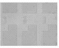
[0057] Step S301, take out the substrate, peel off the photoresist, and obtain such as Figure 4 The array substrate shown.

Embodiment 2

[0059] The manufacturing method of the array substrate of the present invention comprises the following steps:

[0060] Step S101, forming an IGZO oxide material on a substrate to be patterned with an IGZO oxide semiconductor active layer;

[0061] Step S102, forming a photoresist on the substrate after the previous step;

[0062] Step S103, exposing and developing the substrate in the previous step;

[0063] Step S201, soaking the exposed and developed substrate to be patterned with an IGZO oxide semiconductor active layer with water;

[0064] In step S202, acid gas etching is performed on the wetted substrate, the temperature of the acid gas etching solution (DIE A09) is 50° C., and the etching time is 20 s.

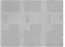
[0065] Step S301, take out the substrate, peel off the photoresist, and obtain such as Figure 5 The array substrate shown.

Embodiment 3

[0067] The manufacturing method of the array substrate of the present invention comprises the following steps:

[0068] Step S101, forming an IGZO oxide material on a substrate to be patterned with an IGZO oxide semiconductor active layer;

[0069] Step S102, forming a photoresist on the substrate after the previous step;

[0070] Step S103, exposing and developing the substrate in the previous step;

[0071] Step S201, soaking the exposed and developed substrate to be patterned with an IGZO oxide semiconductor active layer with water;

[0072] In step S202, acid gas etching is performed on the wetted substrate, the temperature of the acid gas etching solution (DIE A09) is 45° C., and the etching time is 20 s.

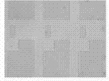
[0073] Step S301, take out the substrate, peel off the photoresist, and obtain such as Figure 6 The array substrate shown.


PUM


Abstract

The invention relates to a manufacture method of an array substrate, which comprises the step of forming a semiconductor active layer pattern, wherein the semiconductor active layer pattern is formed by using an acid gas corrosion etching method. In the manufacture method of the array substrate disclosed by the invention, acidic steam is volatilized through an acidic solution in a container, and an IGZO (Indium Gallium Zinc Oxide) oxide semiconductor layer is etched, so that the uniformity of the etched pattern can be ensured.

Description

technical field [0001] The present invention relates to the field of display technology, in particular to a method for manufacturing an array substrate. Background technique [0002] Wet etching is an essential process step in the TFT (Thin Film Transistor, Thin Film Field Effect Transistor) array manufacturing process, usually gate (Gate) pattern layer and source and drain (S / D) pattern layer and transparent conductive material The pattern layer (usually transparent indium tin oxide) is completed by wet etching process. There are two existing wet etching modes, one is immersion and the other is spray. IGZO (indium gallium zinc oxide, indium gallium zinc oxide) semiconductor is a new film layer, which is a channel layer material used in the new generation of thin film transistor technology. It is a core process in the oxide TFT manufacturing process, replacing The semiconductor active layer (active layer) in the traditional TFT process, and compared with the traditional a-...

Claims


Application Information

Patent Timeline
Patent Type & Authority Applications(China)
IPC IPC(8): H01L21/77
Inventor 赵德江王珂郭炜刘超
Owner BOE TECH GRP CO LTD
Why Eureka
Try Eureka