High light efficiency microchip laser

A microchip laser, high optical efficiency technology, used in lasers, laser parts, phonon exciters, etc., can solve the problems of laser quenching, low optical efficiency and output power, restricting direct application, etc., to improve output power, High pumping efficiency and improved light efficiency

Inactive Publication Date: 2013-01-23
SHANGHAI FEIBO LASER TECH CO LTD
View PDF1 Cites 0 Cited by
  • Summary
  • Abstract
  • Description
  • Claims
  • Application Information

AI Technical Summary

Problems solved by technology

[0004] From the above example, the absorption efficiency of the laser medium for the pump light in the microchip laser structure used by both is about 50%, which directly leads to the low overall light efficiency and output power, which greatly limits its direct application.
[0005] In order to improve the absorption efficiency of pump light, various laser crystals with high doping concentration have been developed, but high-doping laser media generally have problems such as severe thermal effects and laser quenching, which cannot be used for high-power pump applications.

Method used


Image

  • High light efficiency microchip laser
  • High light efficiency microchip laser

Examples


Embodiment 1

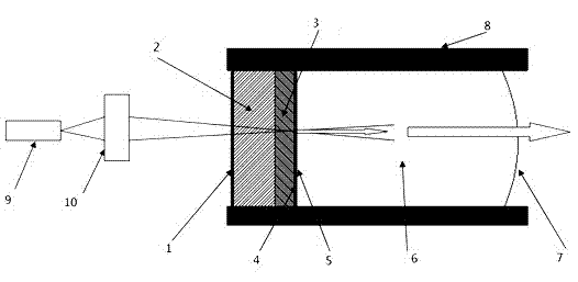
[0025] see first figure 1 , figure 1 It is a schematic structural diagram of Embodiment 1 of the high-efficiency microchip laser of the present invention. It can be seen from the figure that the high-efficiency microchip laser of the present invention includes a pumping light source 9 and a focusing system 10, which are sequentially arranged from left to right along the laser output direction of the pumping light source 9. It is the coupling lens 10, the total reflection cavity film 1, the laser medium 2, the passive Q-switching medium 3, the partial reflection cavity film 4, the first curved surface 5, the amplification medium 6 and the second curved surface 7, in a cylindrical thermal The laser medium 2 and the amplifying medium 6 are sequentially arranged in the 268, and the first curved surface 5 and the second curved surface 7 are two end surfaces of the amplifying medium 6. The first curved surface 5 is a plane, the second curved surface 7 is a spherical surface, R=8mm ...

Embodiment 2

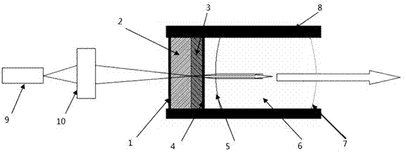
[0028] refer to figure 2 , figure 2 It is a schematic structural diagram of Embodiment 2 of the high optical efficiency microchip laser of the present invention. It can be seen from the figure that the high optical efficiency microchip laser of the present invention includes a pumping light source 9 and a coupling lens 10, which are sequentially arranged from left to right along the laser output direction of the pumping light source 9 It is the coupling lens 10, the total reflection cavity film 1, the laser medium 2, the passive Q-switching medium 3, the partial reflection cavity film 4, the first curved surface 5, the amplification medium 6 and the second curved surface 7, in a cylindrical thermal The laser medium 2 and the amplifying medium 6 are sequentially arranged in the 268, and the first curved surface 5 and the second curved surface 7 are two end surfaces of the amplifying medium 6. The first curved surface 5 is a spherical surface with a radius of curvature R=3mm,...


PUM


Abstract

The invention discloses a high light efficiency microchip laser which comprises a full back cavity mask, a laser medium, a passive Q-adjusting medium (selectable), a partial back cavity mask, a first curve, an amplification medium, a second curve and a heat sink in sequence, wherein after passing through a coupling lens, pump beams emitted by a pump light source income to the laser medium; an optical resonant cavity is formed by the full back cavity mask and the partial back cavity mask; when exceeding the threshold value, the pump light forms continuous pulse laser light to be output. The residual pump light which is not completely absorbed by the laser medium incomes to the amplification medium through the first curve to be absorbed completely; and the whole output power and lighting effect are improved. The second curve has focusing or collimating effects on the output laser light. The heat sink is used for fixing and radiating each device so as to implement modularized package of the whole laser. The laser provided by the invention has the characteristics of simple structure and high pumping efficiency.

Description

technical field [0001] The invention relates to a solid-state laser, in particular to a micro-chip laser with high optical efficiency, and is especially suitable for a short-cavity single-longitudinal-mode micro-chip laser. technical background [0002] Microchip lasers have the advantages of full solidification, small size, simple and compact structure, etc. Because microchip lasers are easy to obtain Q-switched pulses with high repetition rate of sub-nanosecond level, peak power of several thousand watts, and single pulse energy of microjoule level. Therefore, it will have a very wide application prospect in remote measurement, three-dimensional imaging, environmental monitoring, micro-mechanics, micro-surgery, etc. However, since the cavity length of microchip lasers is generally short, especially for short-cavity microchip lasers that produce a single longitudinal mode output, the cavity length is generally less than 1mm, so the volume of the cavity mode is very small, ...

Claims


Application Information

Patent Timeline
IPC IPC(8): H01S3/081H01S3/106H01S3/042
Inventor 彭彪李骁军马昌赞侯晓亮
Owner SHANGHAI FEIBO LASER TECH CO LTD
Why Eureka
Try Eureka