Method for assembling thermo-electric device through printed electronics manufacturing technology

A thermoelectric device and manufacturing process technology, applied in the field of rapid prototyping, to achieve strong controllability, suitable for large-scale production, and a wide range of applications

Inactive Publication Date: 2013-01-30
SHANGHAI UNIV
View PDF7 Cites 9 Cited by
  • Summary
  • Abstract
  • Description
  • Claims
  • Application Information

AI Technical Summary

Problems solved by technology

In addition, it is also possible to print again after the substrate is dried to achieve a multi-layer structure and print complex electronic structures. However, no one has applied the printing method to the assembly of thermoelectric devices.

Method used


Image

  • Method for assembling thermo-electric device through printed electronics manufacturing technology
  • Method for assembling thermo-electric device through printed electronics manufacturing technology
  • Method for assembling thermo-electric device through printed electronics manufacturing technology

Examples


Embodiment 1

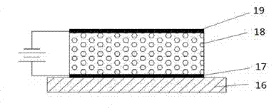
[0028] seefigure 1 with figure 2 , in this example, with Te 2 Bi 3 As a thermoelectric material, those skilled in the art can understand that other known thermoelectric materials can replace Te in the following examples. 2 Bi 3 And realize the technical scheme of this embodiment.

[0029] In this embodiment, the method for assembling a thermoelectric device using a printed electronics manufacturing process includes the following steps:

[0030] First, a bottom electrode is plated on the silicon wafer 16 and the silicon wafer 20;

[0031] Among them, the area of ​​silicon wafer 16 and silicon wafer 20 is 20×20mm 2 , the thickness is 0.5~0.7mm;

[0032] Plating a layer of electrode material on the silicon chip, wherein the electrode material can be Au, Ag, Cu, Zn, Fe, Ni, Pt, Ru, Rh, Pd, Mn or Al, select Cu as the bottom electrode 17 and bottom electrode 17 in this example. Electrode 21 material;

[0033] Next, print n-Te 2 Bi 3 18 or P-Te 2 Bi 3 22 Thermoelectric...

Embodiment 2

[0038] This embodiment is basically the same as Embodiment 1, especially in that:

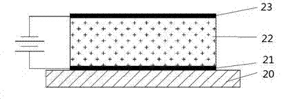
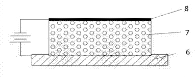
[0039] see image 3 with Figure 4 In this embodiment, the method for assembling thermoelectric devices using a printed electronics manufacturing process includes the following steps:

[0040] First, wet etch the aluminum sheet;

[0041] Among them, the thickness of aluminum sheet 6 and aluminum sheet 9 is 1~2mm, and the area is 20×20mm 2 ;

[0042] The etching depth is selected to be 10~20nm, and the etching area is 15×15mm 2 ;

[0043] Secondly, print n-Te on the aluminum sheet 6 and aluminum sheet 9 2 Bi 3 7 or P-Te 2 Bi 3 10 thermoelectric materials assemble a thermocouple;

[0044] The etched aluminum sheet 6 and aluminum sheet 9 can be used as the bottom electrode of the thermoelectric device, and then print n-Te on the aluminum sheet by screen printing. 2 Bi 3 7 or P-Te 2 Bi 3 10, where the pressure is 0.4~0.6MPa;

[0045] After sintering, weld the top electrode on the...

Embodiment 3

[0049] This embodiment is basically the same as the previous embodiment, and the special features are:

[0050] see Figure 5 In this embodiment, the method for assembling thermoelectric devices using a printed electronics manufacturing process includes the following steps:

[0051] First, a bottom electrode is plated on the silicon wafer 24;

[0052] Wherein, the area of ​​the silicon chip 24 is 20×40mm 2 , the thickness is 0.5~0.7mm;

[0053] Plating a layer of electrode material on the silicon chip, wherein the electrode material can be Au, Ag, Cu, Zn, Fe, Ni, Pt, Ru, Rh, Pd, Mn or Al, select Cu as the bottom electrode 25 material in this example;

[0054] Second, print n-Te on the aluminum sheet 2 Bi 3 26 and P-Te 2 Bi 3 27 thermoelectric materials to assemble a U-shaped thermoelectric device;

[0055] The etched aluminum sheet can be used as the bottom electrode of the thermoelectric device, and then the n-Te 2 Bi 3 26 and P-Te 2 Bi 3 27, where the pressur...


PUM


Abstract

The invention discloses a method for assembling a thermo-electric device through a printed electronics manufacturing technology. The method comprises the steps as follows: directly preparing a thermo-electric size on a bottom electrode in a silk screen printing way; adding the prepared thermo-electric size into a marking press; marking and sintering a substrate to obtain films; drying; then printing or welding a layer of top electrode on the substrate; leading wires from the bottom electrode and the top electrode, so as to assemble to form a thermocouple; and connecting a plurality of thermocouples in series so as to form a thermo-electric device with a large area. By adopting the method, the thermo-electric device can be assembled on a rigid foundation; the thermo-electric device also can be assembled on a flexible base plate such as an aluminum sheet, so that options are diversified; the method is simple, convenient to implement, and low in cost; and compared with conventional preparation technology for thermo-electric devices, the method is high in production efficiency, and particularly suitable for mass production.

Description

technical field [0001] The invention relates to a rapid prototyping method, in particular to an assembly method of thermoelectric devices, which is applied to the field of printing thermoelectric materials on substrates to form films or manufacture devices. Background technique [0002] Thermoelectric devices are a technology that uses the shell effect of semiconductor materials to achieve direct conversion of heat and electricity. It has the characteristics of long life, high reliability and environmental safety. It has broad applications in solar photovoltaic-thermoelectric hybrid power generation and industrial waste heat thermoelectric power generation. Application prospects and potential social and economic benefits. The progress in the assembly of thermoelectric materials has greatly promoted the development of high-performance micro-thermoelectric devices; in turn, the fabrication of micro-thermoelectric devices with various optimized structures is another way to impr...

Claims


Application Information

Patent Timeline
Patent Type & Authority Applications(China)
IPC IPC(8): H01L35/34
Inventor 胡志宇严晓霞肖丹萍
Owner SHANGHAI UNIV
Why Eureka
Try Eureka