Semiconductor device and method of manufacturing the same
A manufacturing method and semiconductor technology, applied in semiconductor/solid-state device manufacturing, semiconductor devices, identification devices, etc., can solve the problems of low reliability and easy changes in electrical characteristics, and achieve high reliability, excellent electrical characteristics, and low cut-off current. Effect
- Summary
- Abstract
- Description
- Claims
- Application Information
AI Technical Summary
Problems solved by technology
Method used
Image
Examples
Embodiment approach 1
[0063] In this embodiment mode, one mode of a semiconductor device and a method of manufacturing the semiconductor device will be described with reference to FIGS. 1A to 7E .
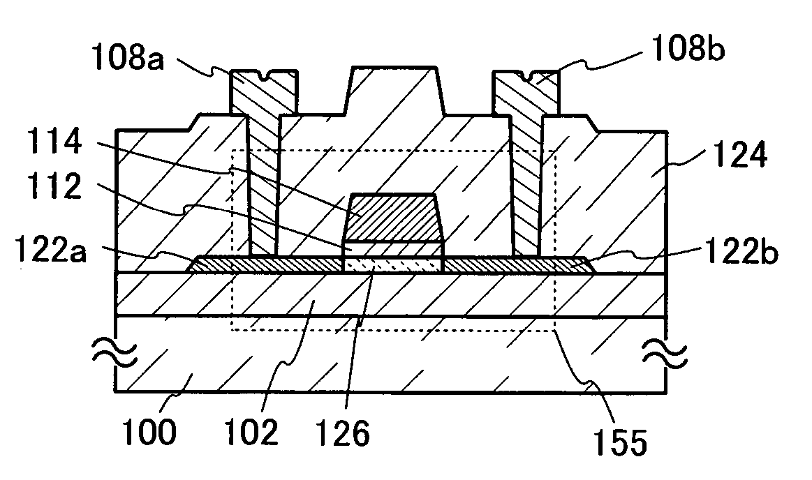
[0064] 1A to 1C show a plan view and a cross-sectional view of a top-gate top-contact transistor 151 as an example of a semiconductor device according to an embodiment of the present invention. Here, FIG. 1A is a plan view, and FIGS. 1B and 1C are cross-sectional views corresponding to the A-B cross-section and the C-D cross-section in FIG. 1A , respectively. Note that, in FIG. 1A , some components of the transistor 151 (for example, the gate insulating layer 112 and the like) are omitted for brevity.
[0065] The transistor 151 shown in FIGS. 1A to 1C includes a base insulating layer 102 , an oxide semiconductor layer 106 , a source electrode 108 a , a drain electrode 108 b , a gate insulating layer 112 , and a gate electrode 114 on a substrate 100 .
[0066] As a material for the insulating base laye...
Embodiment approach 2
[0157] A semiconductor device having a display function (also referred to as a display device) can be manufactured by using the transistor exemplified in Embodiment Mode 1. In addition, a system-on-panel can be formed by forming part or all of a driver circuit including transistors on the same substrate as the pixel portion.
[0158] In FIG. 8A , a sealing material 205 is provided so as to surround a pixel portion 202 provided on a first substrate 201 , and sealing is performed using a second substrate 206 . In FIG. 8A, a scanning line driving circuit formed on a separately prepared substrate using a single crystal semiconductor layer or a polycrystalline semiconductor layer is installed in a region on the first substrate 201 different from the region surrounded by the sealing material 205. 204 . The signal line driving circuit 203 . In addition, various signals and potentials supplied to the separately formed signal line driver circuit 203 , scan line driver circuit 204 , or...
Embodiment approach 3
[0215] The semiconductor device of one embodiment described herein can be applied to various electronic devices (including game machines). Examples of electronic equipment include television sets (also referred to as televisions or television receivers), monitors for computers and the like, video capture devices such as digital cameras and digital video cameras, digital photo frames, and hand-held mobile phones (also referred to as Mobile phones, mobile phone devices), portable game machines, mobile information terminals, sound reproduction devices, large game machines such as pachinko machines, etc. Hereinafter, an example of electronic equipment including the semiconductor device described in the above-mentioned embodiments will be described.
[0216] FIG. 12A shows a notebook personal computer, which is composed of a main body 301, a casing 302, a display unit 303, a keyboard 304, and the like. By applying the semiconductor device shown in Embodiment Mode 1 or 2, a highly ...
PUM
| Property | Measurement | Unit |
|---|---|---|
| length | aaaaa | aaaaa |
| length | aaaaa | aaaaa |
| band gap | aaaaa | aaaaa |
Abstract
Description
Claims
Application Information


