Three-dimensional vacuum sensor and preparation method of three-dimensional vacuum sensor

A technology of vacuum sensor and manufacturing method, which is applied in the fields of vacuum technology and micro-electromechanical systems, can solve the problems of low measurement accuracy, narrow measurement range, and low yield, and achieve the effects of improving sensitivity, increasing gas heat conduction, and improving yield

Active Publication Date: 2013-02-13
SHANGHAI INST OF MICROSYSTEM & INFORMATION TECH CHINESE ACAD OF SCI
View PDF6 Cites 14 Cited by
  • Summary
  • Abstract
  • Description
  • Claims
  • Application Information

AI Technical Summary

Problems solved by technology

[0007] In view of the shortcomings of the prior art described above, the purpose of the present invention is to provide a three-dimensional vacuum sensor and

Method used


Image

  • Three-dimensional vacuum sensor and preparation method of three-dimensional vacuum sensor
  • Three-dimensional vacuum sensor and preparation method of three-dimensional vacuum sensor
  • Three-dimensional vacuum sensor and preparation method of three-dimensional vacuum sensor

Examples


Embodiment 1

[0071] As shown in the figure, the present invention provides a method for preparing a three-dimensional vacuum sensor, the method comprising the following steps:

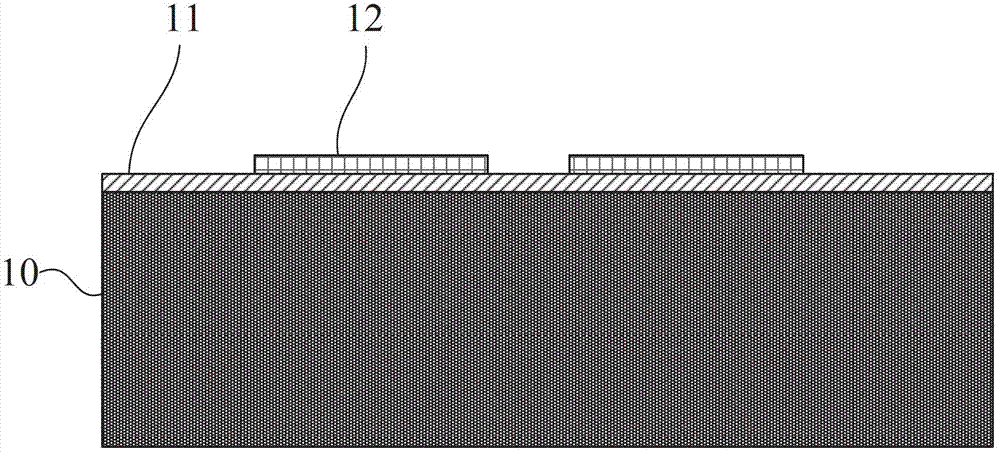
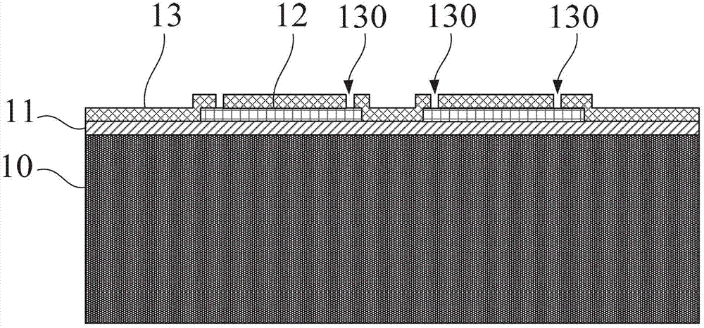
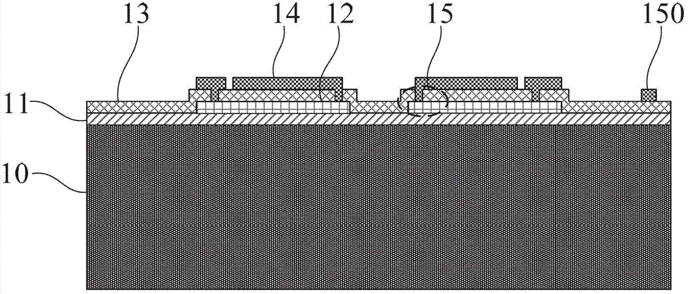
[0072] S1: if Figure 1a As shown, a semiconductor substrate is provided, and the semiconductor substrate can be an SOI substrate, or a common silicon wafer, and the common silicon substrate 10 is tentatively selected in this embodiment. A first silicon oxide layer 11 is prepared as a first dielectric layer on the silicon substrate 10 by a thermal oxidation process, and then a polysilicon layer 12 is deposited on the first silicon oxide layer 11 by an LPCVD process; then ion implantation is used The process dopes the polysilicon layer 12 to make it conductive as the first conductive layer. In other embodiments, the first conductive layer can also be replaced with doped single crystal silicon. The doped ions can be N-type or P-type ions. For example, the commonly used dopants for N-type doping are phosphorus, arsen...

Embodiment 2

[0089] Such as figure 2 As shown, this embodiment provides a structure of a three-dimensional vacuum sensor, including at least: a semiconductor substrate 10', a first supporting film 11', a thermopile (not shown), a second supporting film 12', and a micro heater 13 ' and cover plate 14'.

[0090] The semiconductor substrate 10' has a groove 100', and the semiconductor substrate 10' can be a common silicon substrate or an SOI substrate; the first support film 11' wraps the thermopile, And take the sidewall of the periphery of the groove 100' as support to hang above the groove 100'; the first supporting film 11' is a composite film, and the first supporting film 11' in this embodiment is from bottom to top A composite thin film with a sandwich structure including the first silicon oxide layer 110', the first silicon nitride layer 111', and the second silicon oxide layer 112' in sequence. Better control of dielectric film stress. But it is not limited thereto. In other embo...


PUM

PropertyMeasurementUnit
Thicknessaaaaaaaaaa
Thicknessaaaaaaaaaa

Abstract

The invention provides a three-dimensional vacuum sensor and a preparation method of the three-dimensional vacuum sensor, wherein a thermopile and a heater prepared by the method are located on different planes; the thermopile is located below the heater to further implement miniaturization of a thermoelectric vacuum sensor; a dry etching release structure is utilized to avoid a problem that a structural layer is adhered with a substrate in a wet etching release process, and the yield of devices is improved; a silicon cover board is additionally arranged, that is, gas heat conduction between the cover board and the heater is increased so as to be beneficial to improving sensitivity of a thermal radiation vacuum gauge on an end with higher pressure intensity. In additional, the materials and the preparation process of the semiconductor substrate, the thermopile and the micro heater are all frequently used in the semiconductor process, so the three-dimensional vacuum sensor is easily compatible with an existing CMOS (complementary metal oxide semiconductor) process.

Description

technical field [0001] The invention relates to a sensor and a preparation method thereof, in particular to a three-dimensional heat conduction vacuum sensor and a preparation method thereof, belonging to the technical fields of vacuum technology and micro-electromechanical systems. Background technique [0002] Vacuum measurement has a wide range of applications in the fields of industry, aerospace, and nuclear raw material purification. Traditional vacuum sensors are of various types and large in size, which limits their application in certain fields, especially in some tiny devices and instruments. . Combined with the development history and usage requirements of vacuum sensors, the current commonly used vacuum gauges have a tendency to develop in the direction of miniaturization, integration, systematization and intelligence. The rapid development of MEMS, especially the rapid development of micro-processing technology, has made the development of miniaturization of vac...

Claims


Application Information

Patent Timeline
IPC IPC(8): G01L21/10B81B7/00B81C1/00
Inventor 熊斌孙晓徐德辉王跃林
Owner SHANGHAI INST OF MICROSYSTEM & INFORMATION TECH CHINESE ACAD OF SCI
Why Eureka
Try Eureka