A radio frequency single electron transistor scanning probe and its application

A single-electron transistor and scanning probe technology, which is used in the field of radio-frequency single-electron transistors to make scanning probes, charge scanning imaging, and oscilloscope and atomic force imaging systems, can solve the problem of inability to perform spatial scanning, large mutual influence, and inability to charge Signal effective test and other problems, to achieve the effect of high sensitivity, high charge detection, wide operating temperature range

Active Publication Date: 2014-10-08
SUZHOU INST OF NANO TECH & NANO BIONICS CHINESE ACEDEMY OF SCI
View PDF2 Cites 0 Cited by
  • Summary
  • Abstract
  • Description
  • Claims
  • Application Information

AI Technical Summary

Problems solved by technology

The charge sensitivity of the above-mentioned single-electron transistor probe has reached 10 -5 e / Hz 0.5 charge sensitivity; but the speed is lower than 100kHz, and it is not yet possible to effectively test the charge signal on the order of microseconds and nanoseconds; based on Al / Al 2 o 3 type single-electron transistor, the operating temperature is usually below 300mK; there is no control gate on the probe, and the operating point of the transistor is set by the circuit under test, which greatly affects each other
The above-mentioned radio frequency single-electron transistor has the characteristics of high speed and high sensitivity, and the bandwidth is as high as 100MHz; but because it is fixed on the substrate, it cannot be used for spatial scanning; the Al / Al based 2 o 3 Or GaAs / AlGaAs single-electron transistors, the operating temperature is usually below 300mK

Method used


Image

  • A radio frequency single electron transistor scanning probe and its application
  • A radio frequency single electron transistor scanning probe and its application
  • A radio frequency single electron transistor scanning probe and its application

Examples


Embodiment Construction

[0021] The invention forms a radio frequency single electron transistor scanning probe by integrating a single electron transistor and a radio frequency resonance circuit, and forms a system of charge scanning imaging, oscilloscope and atomic force appearance imaging with the support of peripheral systems.

[0022] The technical solution of the present invention will be further described below in conjunction with the accompanying drawings and a preferred embodiment.

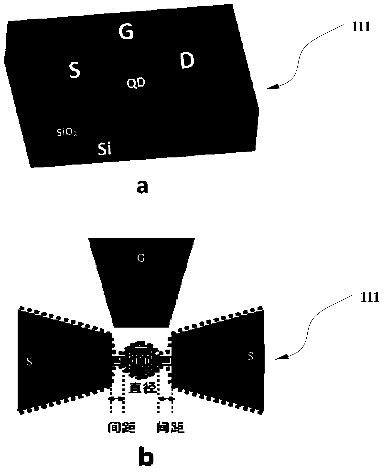
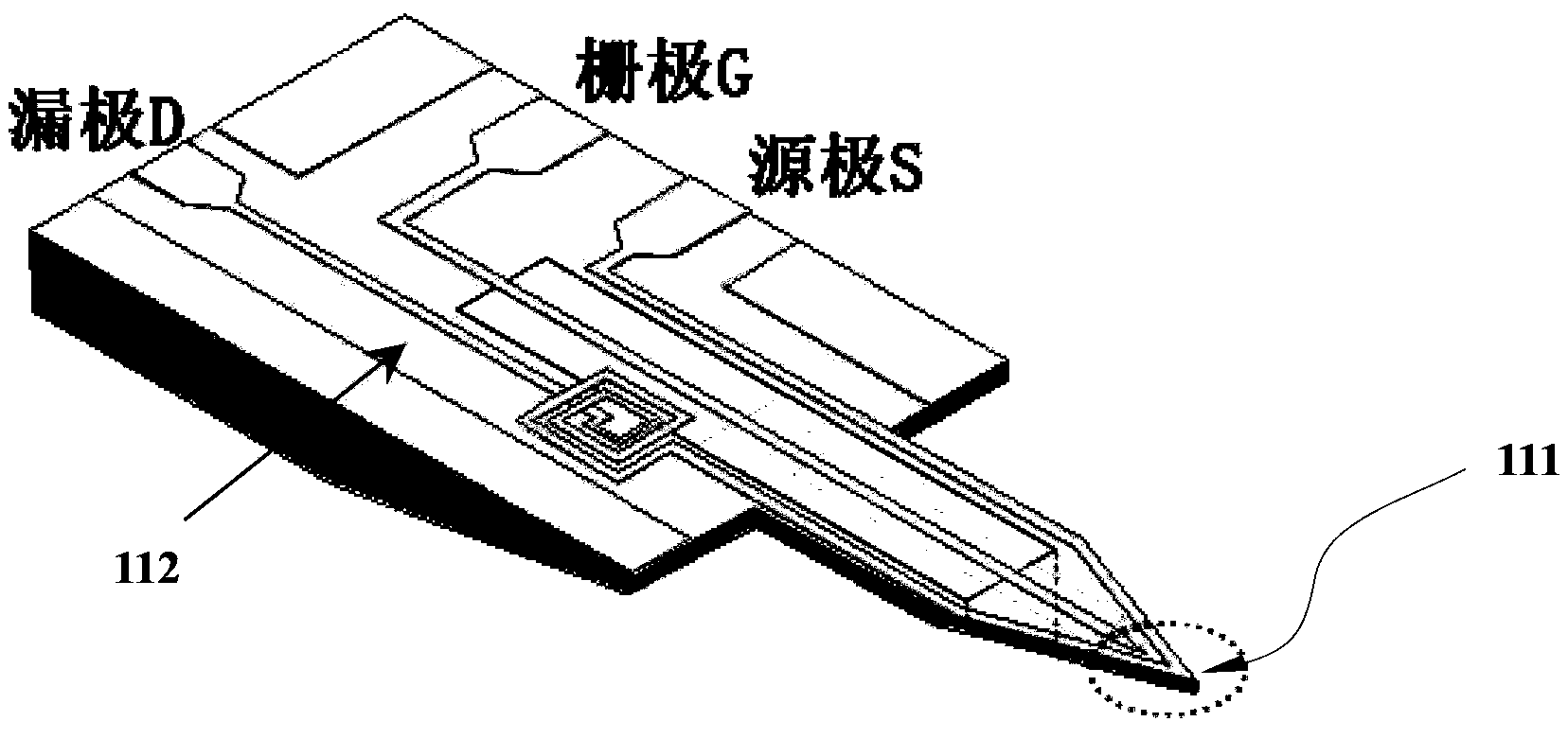
[0023] like image 3 As shown, the integrated radio frequency single-electron transistor scanning probe (RF-SET Scanning Probe) includes an SOI substrate, and one end of the SOI substrate is a needle-shaped protrusion. The SOI is provided with a matching radio frequency resonance circuit and a single-electron transistor, wherein the single-electron transistor is integrated on the needle-shaped protrusion of the SOI substrate, and the radio frequency resonance circuit is integrated on the root body of the SOI subs...


PUM


Abstract

The invention relates to a nanometer device and a nanometer machining technology, in particular to the structure of a radio-frequency single-electron transistor scanning probe and application thereof. The radio-frequency single-electron transistor scanning probe comprises an SOI (silicon on insulator) substrate of which one end has a needle-shaped lug boss, and a radio-frequency resonant circuit and a single-electron transistor integrated on the SOI substrate and matched with each other; and the single-electron transistor is integrated on the needle-shaped lug boss of the SOI. The invention further provides a manufacture method of the radio-frequency single-electron transistor scanning probe and a charge scanning imaging and oscillography and atomic power showing imaging system manufactured by the radio-frequency single-electron transistor scanning probe. The system is high in sensitivity, high in speed and high in spatial resolution, can form into the distribution morphology and the geometric morphology of the charge by means of low-temperature three-dimensional scanning, and can detect the electric potential and the dynamic change of the electric potential at any one point in the nanometer device or circuit at fixed points.

Description

technical field [0001] The invention relates to a nano device and a nano processing technology, especially a technology for making a scanning probe with an integrated radio frequency single electron transistor, which can also be applied to charge scanning imaging, oscillometric and atomic force imaging systems. Background technique [0002] Single-electron transistors based on the Coulomb blocking effect and single-electron tunneling effect have extremely high sensitivity to small charge changes in their neighborhoods at the micro-nano scale. The core of single-electron transistors sensitive to charges is quantum dots or Coulomb islands with a scale of only a few to tens of nanometers. The quantum dots are coupled to the source and drain electrodes through the tunneling barrier, and the control gate and the Coulomb islands are coupled through capacitive coupling. Single-electron transistors can be used for fixed-point high-sensitivity charge detection at the micro-nano scale...

Claims


Application Information

Patent Timeline
Patent Type & Authority Patents(China)
IPC IPC(8): G01Q60/38G01Q60/30
Inventor 吕利秦华李欣幸孙建东张晓渝
Owner SUZHOU INST OF NANO TECH & NANO BIONICS CHINESE ACEDEMY OF SCI
Why Eureka
Try Eureka