Silicon on insulator (SOI)-based opto-isolator based on symmetrical vertical grating coupling structure

A vertical grating and vertical coupling technology, applied in the direction of coupling of optical waveguides, can solve the problems of inability to achieve monolithic integration, incompatible manufacturing processes, and restricting optical interconnection.

Inactive Publication Date: 2013-02-13
INST OF SEMICONDUCTORS - CHINESE ACAD OF SCI
View PDF3 Cites 11 Cited by
  • Summary
  • Abstract
  • Description
  • Claims
  • Application Information

AI Technical Summary

Problems solved by technology

The traditional optical isolator is bulky and expensive, and the manufacturing process is not compatible with the CMOS process, and cannot be monolithically integrated, which also restricts the realization of optical interconnection

Method used


Image

  • Silicon on insulator (SOI)-based opto-isolator based on symmetrical vertical grating coupling structure
  • Silicon on insulator (SOI)-based opto-isolator based on symmetrical vertical grating coupling structure
  • Silicon on insulator (SOI)-based opto-isolator based on symmetrical vertical grating coupling structure

Examples


Embodiment Construction

[0018] specific implementation plan

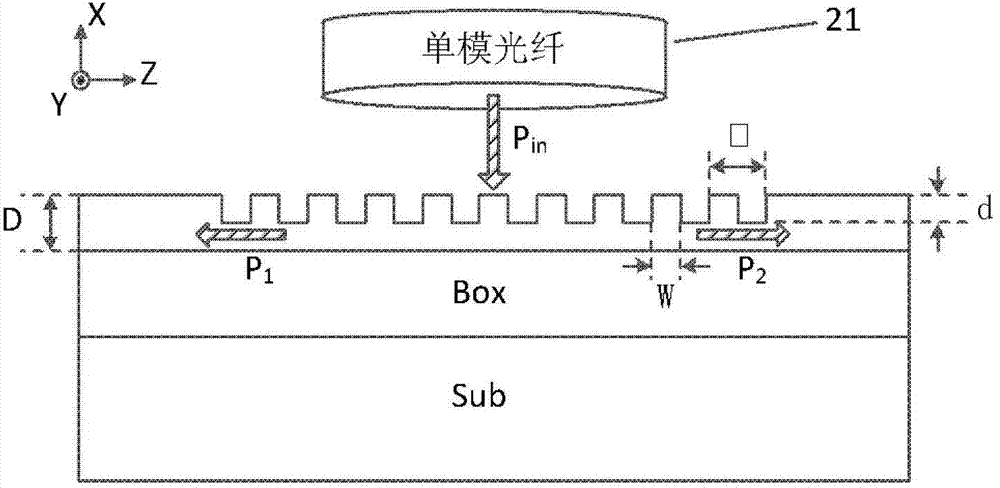
[0019] Because the present invention is a silicon-based optical isolator based on SOI substrate material design, for different buried oxide layer thicknesses and top-layer silicon thicknesses, the corresponding optimal design is also different in order to achieve functional requirements. Therefore, for convenience of description, the substrate of the present invention The bottom material defaults to specific implementation parameters, that is, the thickness of the buried oxide layer is 2 μm, and the thickness of the top silicon layer is 220 nm.

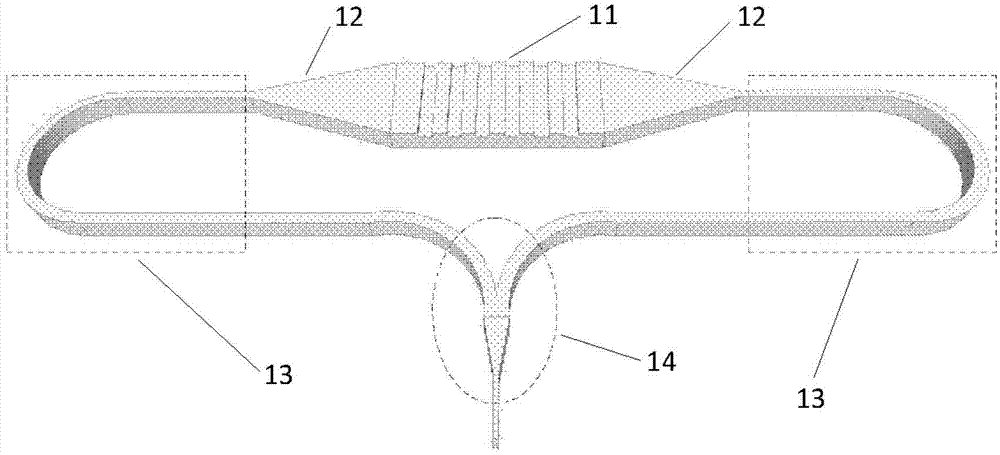
[0020] figure 1 For a three-dimensional schematic diagram of a specific embodiment of the present invention, refer to figure 1 As shown, the present invention provides a kind of SOI-based optical isolator based on symmetrical vertical grating coupling structure, comprising:

[0021] A vertical coupling grating 11, the vertical coupling grating 11 is a symmetrical vertical coupling grating 1;

...


PUM


Abstract

The invention discloses a silicon on insulator (SOI)-based opto-isolator based on a symmetrical vertical grating coupling structure. The structure comprises a vertical coupling grating, two mode converters which are manufactured on two sides of the vertical coupling grating respectively to realize approximately loss-free energy transmission and mode conversion, two single-mode ridge waveguides which are connected with one ends of the two mode converters respectively, and an optical beam combiner which is connected with the other ends of the two single-mode ridge waveguides respectively, wherein the vertical coupling grating, the two mode converters, the two single-mode ridge waveguides and the optical beam combiner are manufactured on one substrate. The opto-isolator has the advantages of integration of coupling and optical isolation functions, simplicity in alignment, low insertion loss and compatibility of a manufacturing process and a complementary metal oxide semiconductor (CMOS) process, and is expected to be applied to a future on-chip / inter-chip optical interconnection network.

Description

technical field [0001] The invention relates to silicon-based photonics and chip-level optical interconnection technology, in particular to an SOI-based optical isolator based on a symmetrical vertical grating coupling structure. Background technique [0002] In the past half century, with the development of integrated circuits, silicon-based materials and device technology have been very mature, and with the continuous reduction of process feature size, the integration of integrated circuits has been developing rapidly in accordance with Moore's law. The higher integration of chips brings not only an increase in the number of transistors, but also an increase in chip functions and processing speed. However, as feature sizes shrink and integration levels continue to increase, the limitations of microelectronics processes are becoming increasingly apparent. Although the delay and power consumption of individual transistors are getting smaller and smaller, the delay and power...

Claims


Application Information

Patent Timeline
IPC IPC(8): G02B6/26
Inventor 黄北举张赞张赞允陈弘达
Owner INST OF SEMICONDUCTORS - CHINESE ACAD OF SCI
Why Eureka
Try Eureka