Visualization detection method of electronic product electronic design automation (EAD) design manufacturability

A technology for electronic products and detection methods, applied in the fields of computing, electrical digital data processing, special data processing applications, etc., can solve problems such as the inability to solve various practical problems of enterprises, single practical problems of enterprises, etc., to solve the problem of inconsistent file coordinates, improve Efficiency and quality, the effect of reducing the number of trial runs and adjustments

Active Publication Date: 2013-02-13
CHANGZHOU AUTOSMT INFORMATION TECH
View PDF2 Cites 29 Cited by
  • Summary
  • Abstract
  • Description
  • Claims
  • Application Information

AI Technical Summary

Problems solved by technology

[0003] At present, DFM design manufacturability technology is being developed at home and abroad, which can only solve a single practical problem of the enterprise (such as PCB assembly), but cannot solve various practical problems of the enterprise, let alone 3D visual flickering display of specific errors on the virtual PCB The position and type of the product need repeated trial production and adjustment

Method used


Image

  • Visualization detection method of electronic product electronic design automation (EAD) design manufacturability
  • Visualization detection method of electronic product electronic design automation (EAD) design manufacturability
  • Visualization detection method of electronic product electronic design automation (EAD) design manufacturability

Examples


Embodiment 1)

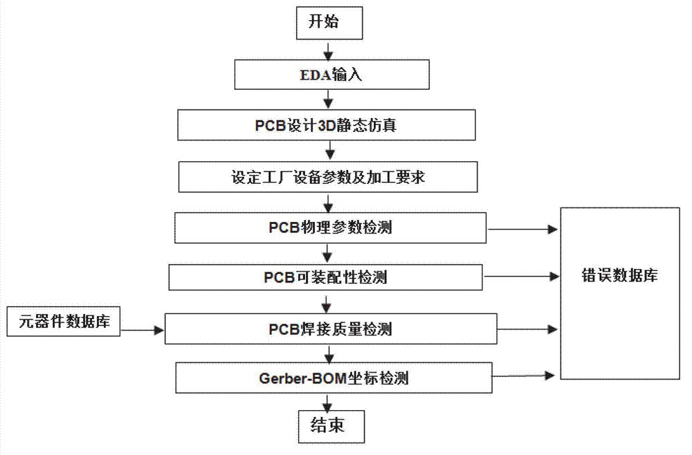
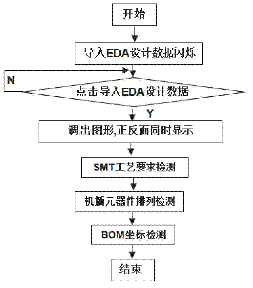
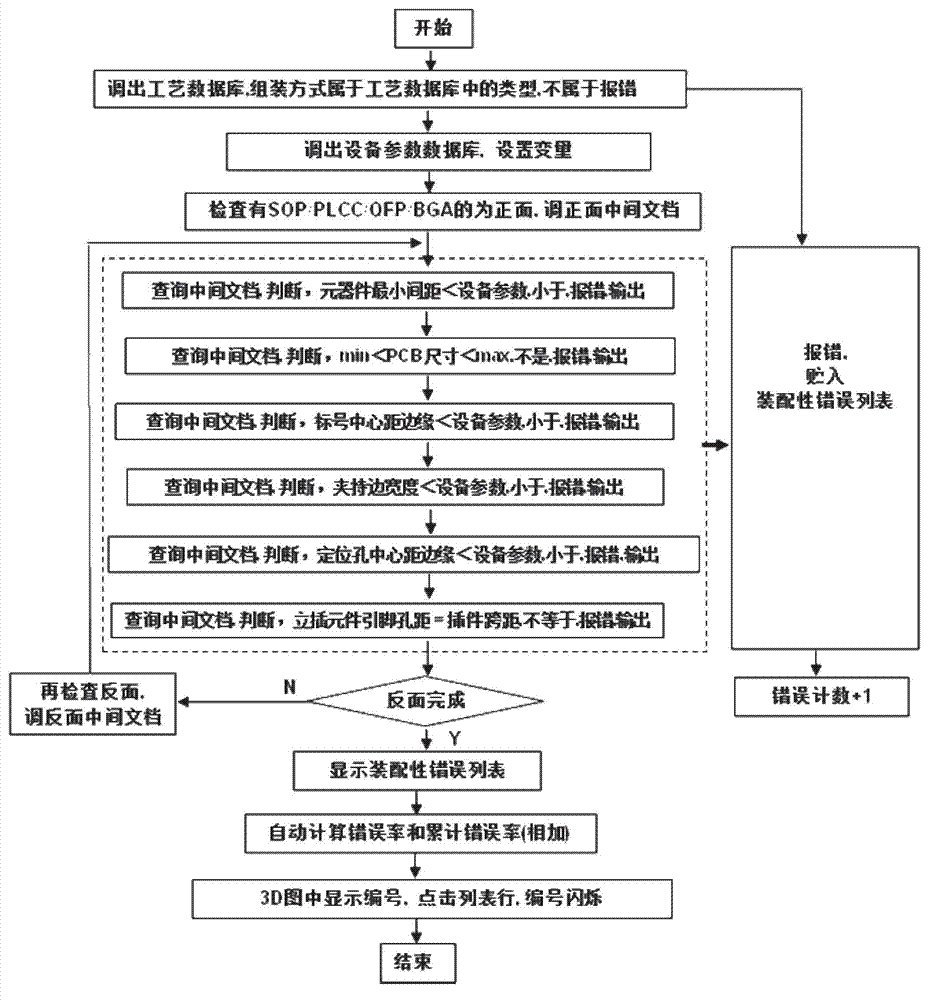
[0055] See figure 1 , the electronic product EDA design manufacturability visual detection method of the present embodiment, carry out PCB 3D simulation to EDA design file, then carry out PCB physical parameter detection detection, PCB assembleability detection, PCB soldering quality detection and Gerber BOM coordinate detection sequentially , and 3D visually display the specific error locations and types of the aforementioned four detections on the PCB 3D simulation graphics. Generally speaking, the following steps are included:

[0056] Step 1: EDA input: extract information from the EDA design file or Gerber file, and convert it into a PCB intermediate file with a unified format; the specific method is: extract the component information and pad information of the EDA design file, and convert it into a virtual simulation The virtual EDA file EDASim.txt; then extract the component information of the Gerber file and BOM file respectively, and convert it into a virtual simulat...


PUM


Abstract

The invention discloses a visualization detection method of electronic product electronic design automation (EDA) design manufacturability. Printed circuit board (PCB) three dimensional (3D) simulation of an EDA design document is conducted, PCBphysical parameter detection, PCB assembling ability, PCB welding quality detection and Gerber bill of material (BOM) coordinate detection are conducted in sequence, and specific error positions and types of former four steps of detection are displayed in visualization mode on a PCB 3D figure. On the basic of complete actual production experiences, the visualization detection method and a system of the EAD design manufacturability are developed according to international standard of information processing center (IPC), the PCB physical parameter detection, the PCB assembling ability, the PCB welding quality detection and the gerber BOM coordinate detection which are all designed by EDA are integrated, the various actual problems which are the contradictions of manufacture and design of PCB and are faced by enterprises are resolved, and efficiency and quality of electronic manufacture in particular to an original equipment manufacturer (OEM) are improved.

Description

technical field [0001] The invention relates to a visual detection method for EDA design manufacturability of electronic products. Background technique [0002] More than 50% of the quality problems in the production of electronic products are caused by design errors. For example, Sichuan Changhong Precision Electronic Technology Co., Ltd. assembles and manufactures more than 4,000 kinds of PCB boards every year, and about 50% of the PCB boards have design errors. In the SMT surface assembly production of electronic products, electronic designers generally use computer-aided design EDA tools (such as Protel, PowerPCB, OrCAD, Candence, Mentor) to complete PCB design. However, electronic designers do not understand the manufacturability requirements of modern electronic mass production and the production process of specific production lines, so design errors often occur, and the errors are not discovered until the electronic products are trial-produced, and then repeatedly mod...

Claims


Application Information

Patent Timeline
Patent Type & Authority Applications(China)
IPC IPC(8): G06F17/50
Inventor 龙绪明黄昊贾建军钟劫李巍俊张治敏杨飞任伯宇闫明严如俊崔晓璐
Owner CHANGZHOU AUTOSMT INFORMATION TECH
Why Eureka
Try Eureka