IGBT (Insulated Gate Bipolar Transistor) device with field stop buffer layer and manufacture method of IGBT device

A manufacturing method and buffer layer technology are applied in the direction of semiconductor/solid-state device manufacturing, semiconductor devices, electrical components, etc., to achieve the effects of improving conduction characteristics, increasing current density, and increasing thickness

Active Publication Date: 2015-06-10
HANGZHOU SILAN INTEGRATED CIRCUIT
View PDF4 Cites 0 Cited by
  • Summary
  • Abstract
  • Description
  • Claims
  • Application Information

AI Technical Summary

Problems solved by technology

However, in the application process of the entire IGBT device, since the thickness of the field stop N-type buffer layer is between 2-10um, the problem that its conduction loss accounts for a large proportion has become increasingly prominent, and can no longer be used neglect

Method used


Image

  • IGBT (Insulated Gate Bipolar Transistor) device with field stop buffer layer and manufacture method of IGBT device
  • IGBT (Insulated Gate Bipolar Transistor) device with field stop buffer layer and manufacture method of IGBT device
  • IGBT (Insulated Gate Bipolar Transistor) device with field stop buffer layer and manufacture method of IGBT device

Examples


Embodiment Construction

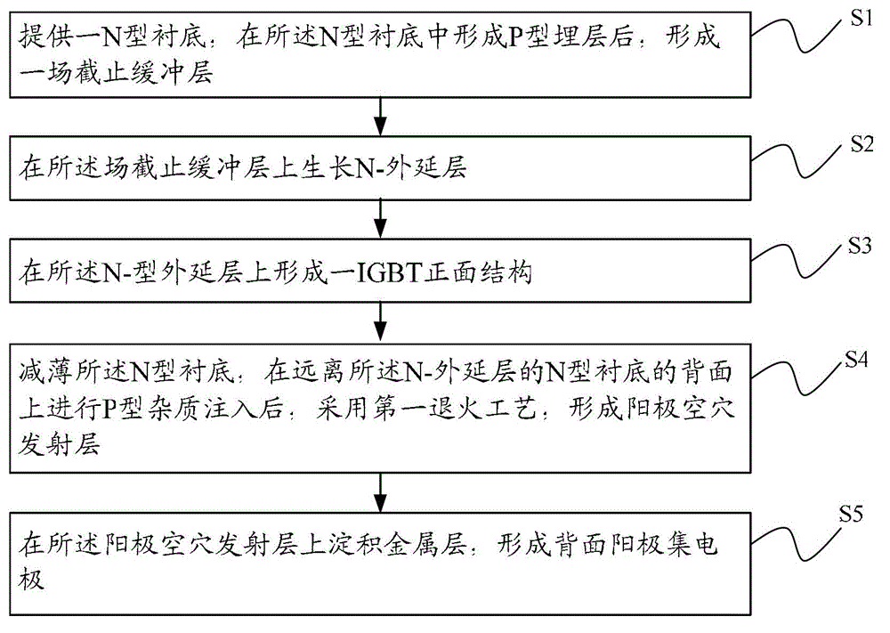
[0049] In order to make the above objects, features and advantages of the present invention more comprehensible, specific implementations of the present invention will be described in detail below in conjunction with the accompanying drawings.

[0050] In the following description, numerous specific details are set forth in order to provide a thorough understanding of the present invention. However, the present invention can be implemented in many other ways different from those described here, and those skilled in the art can make similar extensions without violating the connotation of the present invention, so the present invention is not limited by the specific implementations disclosed below.

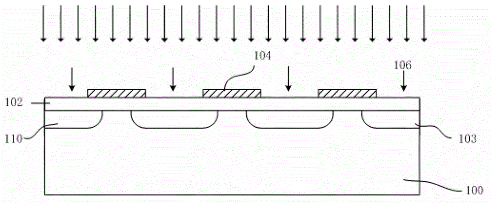
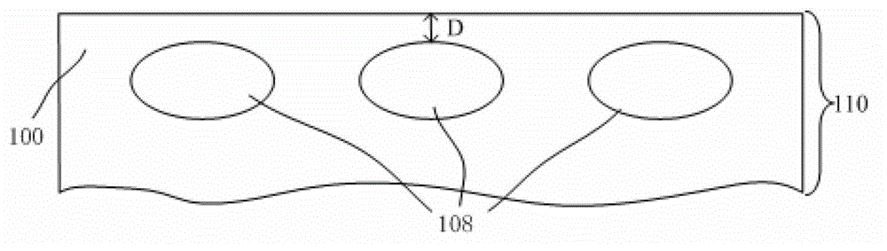
[0051] see Figure 7, the present invention provides a field stop buffer layer formed in an IGBT device, comprising: an N-type substrate 100 ; and a P-type buried layer 108 formed in the N-type substrate 100 .

[0052] see Figure 7 , the present invention also provides an IGBT de...


PUM


Abstract

The invention provides a field stop buffer layer which is formed in an IGBT (Insulated Gate Bipolar Transistor) device. The field stop buffer layer comprises an N type substrate and a P type buried layer formed in the N type substrate. The invention also provides an IGBT device with the field stop buffer region. The IGBT device comprises the field stop buffer layer, an N-epitaxial layer, an IGBT front structure, an anode cavity emission region and a back anode collector electrode, wherein the field stop buffer layer comprises the N type substrate and the P type buried layer formed in the N type substrate; the N-epitaxial layer is formed on the surface of the N type substrate; the IGBT front structure is formed on the surface of the N-epitaxial layer; the anode cavity emission region is formed on the back surface, which is far away from the N-epitaxial layer, of the N type substrate; and the back anode collector electrode is formed on the anode cavity emission region. The invention also provides a manufacture method of the IGBT device with the field stop buffer layer. Through increasing the thickness of the field stop buffer layer and regulating the concentration and the thickness between the P type buried layer and the N type substrate, the current density of the IGBT device is increased, and the conduction loss is reduced.

Description

technical field [0001] The invention belongs to the technical field of power semiconductor devices, in particular to an IGBT device with a field stop buffer layer and a manufacturing method. Background technique [0002] Insulated gate bipolar transistor (IGBT) is a commonly used power switching device controlled by voltage. It has large input capacitance, high input impedance, small driving current, fast speed, high withstand voltage, strong thermal stability, and high operating temperature. , Simple control circuit and other characteristics, it has become the mainstream device of power electronic devices at this stage. [0003] Since the invention of IGBT devices in the 1980s, they have experienced a series of evolutions such as PT (punch-through) type, PT (punch-through) type with N+ buffer layer, and NPT (non-punch-through) type and other field-stop (FS) IGBTs. The thickness of the IGBT chip has also been reduced from the initial 300um to the current 70um, and the chip ...

Claims


Application Information

Patent Timeline
Patent Type & Authority Patents(China)
IPC IPC(8): H01L29/739H01L29/06H01L21/331
CPCH01L29/66333H01L29/0834H01L29/7395
Inventor 顾悦吉闻永祥刘琛刘慧勇
Owner HANGZHOU SILAN INTEGRATED CIRCUIT
Why Eureka
Try Eureka