Light-emitting diode of photonic crystal structure and application thereof

A technology of light-emitting diodes and photonic crystals, applied in semiconductor devices, electrical components, circuits, etc., can solve the problems of low luminous efficiency and low light extraction efficiency of GaN-based LEDs, and achieve the effect of improving light-emitting efficiency and reducing ohmic contact resistance.

Active Publication Date: 2013-02-27
SOUTHEAST UNIV
View PDF4 Cites 21 Cited by
  • Summary
  • Abstract
  • Description
  • Claims
  • Application Information

AI Technical Summary

Problems solved by technology

[0012] Technical problem: In view of the problems and deficiencies in the above-mentioned existing GaN-based LEDs with photonic crystal structures and their preparation methods, a light-emitting diode with a photonic crystal structure provided by the present invention can not only solve the problem of existing GaN-based LEDs The problem of low composite luminous efficiency and light extraction efficiency of LED can avoid the damage caused by the introduction of photonic crystals to the p-type GaN layer and the active region of the LED.

Method used


Image

  • Light-emitting diode of photonic crystal structure and application thereof
  • Light-emitting diode of photonic crystal structure and application thereof
  • Light-emitting diode of photonic crystal structure and application thereof

Examples


Embodiment Construction

[0028] The present invention will be further described below in conjunction with the accompanying drawings.

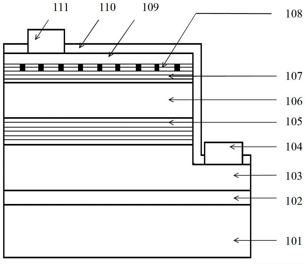
[0029] like figure 1 Shown is a side view of an LED with a novel photonic crystal structure provided by the present invention. The structural elements of the LED include: substrate 101, buffer layer 102, n-type GaN epitaxial layer 103, n-type electrode 104, active light-emitting layer 105 of InGaN / GaN multiple quantum wells, p-type GaN epitaxial layer 106, p-type superstructure The lattice structure 107 , the photonic crystal structure 108 prepared in the p-type superlattice structure 107 , the transparent conductive layer 109 , the passivation layer 110 , and the p-type electrode 111 .

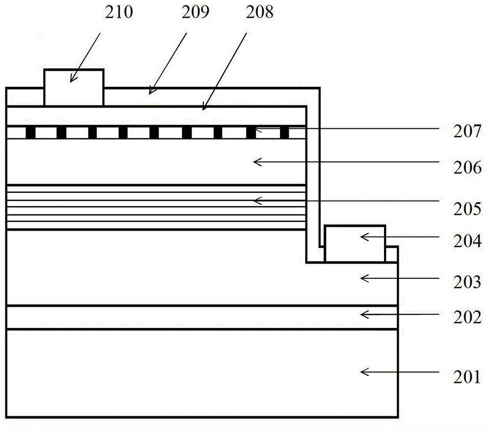
[0030] like figure 2 Shown is a side view of a prior art LED with a photonic crystal structure. Its constituent elements include: substrate 201, buffer layer 202, n-type GaN epitaxial layer 203, n-electrode 204, InGaN / GaN multiple quantum well active light-emitting layer 205, p-ty...


PUM


Abstract

The invention provides a light-emitting diode of a photonic crystal structure. The light-emitting diode is provided with a substrate (101), a buffer layer (102), an n-type GaN epitaxial layer (103), an active luminescent layer (105) with InGaN / GaN multiple quantum wells, a p-type GaN epitaxial layer (106), a p-type super-lattice structure (107), a transparent conducting layer (109) and a passivation layer (110) in sequence from bottom to top, wherein an n-type electrode (104) is further arranged on the n-type GaN epitaxial layer (103); a p-type electrode (111) is further arranged on the transparent conducting layer (109); and a photonic crystal structure (108) is prepared in the p-type super-lattice structure (107). The light-emitting diode is applicable to a GaN-based LED (Light-emitting Diode), and is also applicable to other photo-electronic apparatuses which need to improve reflectivity of a certain wave band.

Description

technical field [0001] The invention belongs to the technical field of semiconductor optoelectronic device manufacturing, and mainly relates to a photonic crystal structure fabricated in a superlattice of an LED. Manufacturing technology for LED light extraction efficiency. Background technique [0002] LEDs are the most widely used active devices in the current electronic information industry, and high-brightness LEDs only release a small amount of heat in the energy conversion process. It has better application prospects. [0003] With the improvement of epitaxial growth technology, the brightness and efficiency of GaN-based LEDs have been significantly improved. However, in order to realize high-performance LED devices, it is crucial to further improve the quality of the p-type GaN layer. Researchers have verified experimentally [1] that the introduction of a superlattice structure on the surface of GaN-based LEDs can increase the electron-hole recombination luminous e...

Claims


Application Information

Patent Timeline
Patent Type & Authority Applications(China)
IPC IPC(8): H01L33/04H01L33/20H01L33/00
Inventor 张雄王春霞陈洪钧崔一平
Owner SOUTHEAST UNIV
Why Eureka
Try Eureka