Process for welding electronic microcomponents based on multi-temperature gradient

A process method and micro-component technology, applied in welding equipment, manufacturing tools, metal processing equipment, etc., can solve the problems of less welding temperature steps, difficult quantitative flaw detection, and low multi-functional integration, so as to achieve less welding voids and avoid Detection problems, stable and reliable processing quality

Inactive Publication Date: 2013-03-06
10TH RES INST OF CETC
View PDF4 Cites 18 Cited by
  • Summary
  • Abstract
  • Description
  • Claims
  • Application Information

AI Technical Summary

Problems solved by technology

[0005] The purpose of the present invention is to address the problems in the prior art above, and provide a simple, convenient, high-efficiency, stable and reliable processing quality, good welding fluidity, and less welding voids. There are few welding temperature steps for electronic TR components, low multi-functional integration, limited thermal expansion mismatch of lightweight materials, poor stability and consistency of welding indicators, and difficult quantitative flaw detection.

Method used


Image

  • Process for welding electronic microcomponents based on multi-temperature gradient
  • Process for welding electronic microcomponents based on multi-temperature gradient
  • Process for welding electronic microcomponents based on multi-temperature gradient

Examples


Embodiment Construction

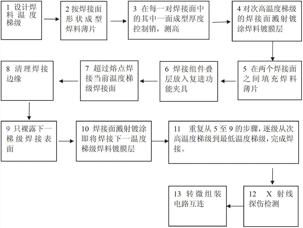
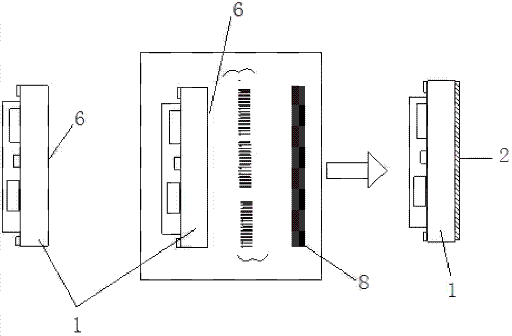
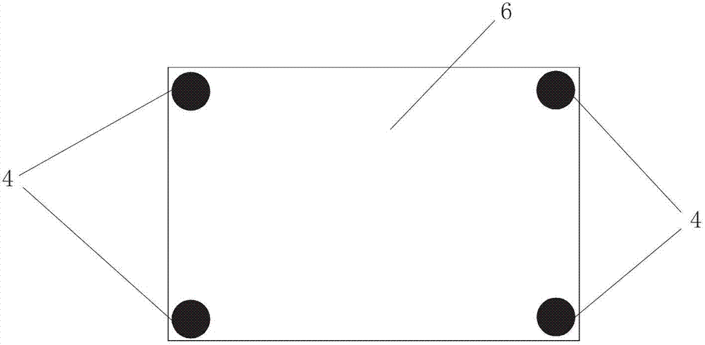
[0030] refer to figure 1 . The target material 8 is the source of the physical coating material. Different target materials have different melting point temperatures and components. The melting point and composition of the formed welding surface coating layer 2 are exactly the same as the melting point and composition of the solder sheet 3 material corresponding to the melting point temperature. The coating layer on the soldering surface of the electronic micro-component 1 and the solder thin sheet 3 are all the same component material. The highest temperature welding has no limit on the upper limit of temperature rise, so the temperature can be raised to solve the solderability problem. The base assembly 5 is a relative concept. For the microelectronic assembly 12, it is the bond connected with the TR assembly cavity 11. For the TR assembly, it refers to the final packaging shell of the entire assembly; the shape of the solder sheet 3 is completely consistent with the shape ...


PUM

PropertyMeasurementUnit
thicknessaaaaaaaaaa

Abstract

The invention discloses a process for welding electronic microcomponents based on a multi-temperature gradient. The process is simple, convenient, efficient, stable and reliable in processing quality, good in welding flowability and little in welding hollows. The process is realized by the following technical scheme: designing the temperature gradient of welding fluxes according to melting points of different welding fluxes and respectively manufacturing welding flux slices at different temperature gradients from a secondary high temperature to a minimum temperature; dividing a function substrate and a transition parent plate on each electronic microcomponent into welding surfaces of the welding fluxes at different temperature gradients and coating a welding flux film coating layer on the welding surfaces directly and respectively by sputter coating; arranging welding flux thickness control pins at more points on the welding surfaces of the electronic component; laminating the electronic microcomponents (1), the welding flux slices (3) and the substrate component (5) sequentially, putting into a clamp with a counter-recoil pressure holding mechanism and putting the clamp into a furnace for vacuum welding; firstly completing the welding at a high temperature gradient, and then protecting other surfaces, which are not used for the welding at the next temperature gradient, of the substrate component, and coating one welding flux film coating layer on the welding surfaces respectively by the sputter coating at the next temperature gradient.

Description

technical field [0001] The invention relates to a process method for multi-temperature cascade welding of electronic micro-components, in particular to a micro-assembly process method that requires high-precision temperature control and welding of electronic micro-components to be integrated into electronic components. Background technique [0002] In the micro-assembly process of multi-functional electronic components, welding involves the reliability and quality of the product, which directly affects the electrical performance index of the product and the product environmental adaptability assessment and acceptance review. In addition, due to the rapid development of electronic components in the direction of lightness, thinness and smallness, a series of welding process problems have been raised. For this reason, manufacturers of complete electronic equipment have launched fierce competition around the welding process of electronic components, especially TR components. Fur...

Claims


Application Information

Patent Timeline
Patent Type & Authority Applications(China)
IPC IPC(8): B23K1/008B23K1/20
Inventor 詹为宇
Owner 10TH RES INST OF CETC
Why Eureka
Try Eureka