

Copper foil substrate for flexible printed circuit boards
A flexible printing and copper foil substrate technology, which is applied in the direction of circuit substrate materials, printed circuit components, layered products, etc., can solve problems such as complicated production procedures, easy-to-interpret circuit design distribution, and affect product market sales and company operations. , to achieve the effect of high heat dissipation, high brightness and heat dissipation
- Summary
- Abstract
- Description
- Claims
- Application Information
AI Technical Summary
Problems solved by technology
Method used
Image

Examples
Embodiment 1
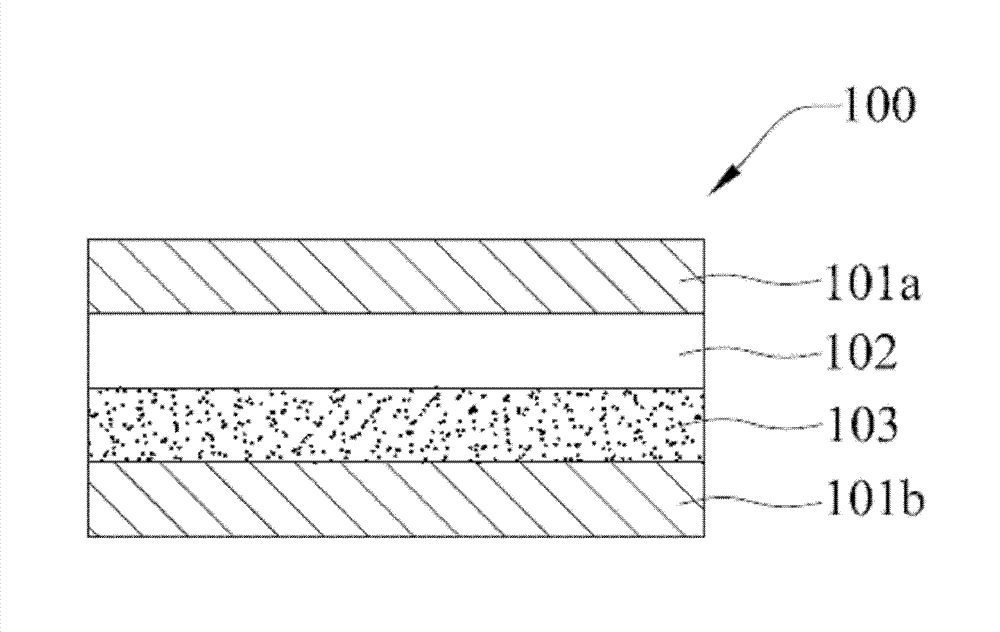
[0025] Example 1: figure 1 Shown is the copper foil substrate 100 for a flexible printed circuit board according to Embodiment 1 of the present invention, which is presented in the form of a double panel. The copper foil substrate 100 is provided with a first copper foil 101a, a polyimide layer 102, a second A reflective layer 103 and a second copper foil 101b.
[0026] The first copper foil 101a and the second copper foil 101b in this example can be electrolytic copper foil or rolled copper foil, and generally, the thicknesses of the first copper foil 101a and the second copper foil 101b can be between 9 and 35 microns, and the thickness difference between the first copper foil and the second copper foil is less than 26 microns.
[0027] In order to reduce the light transmittance and incomplete heat dissipation of the flexible circuit boards produced, the copper foil substrate of the present invention obtains a thinner but more flexible circuit board by adjusting the thickne...
Embodiment 2
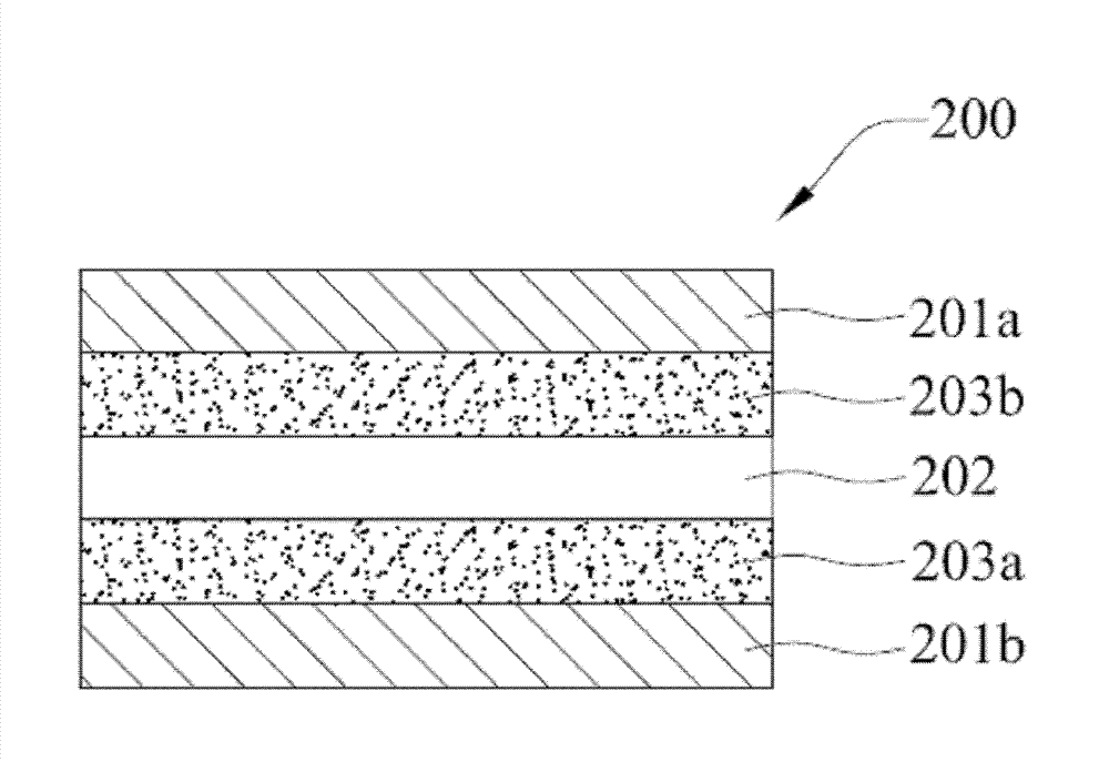
[0035] Example 2: figure 2 Shown is the flexible printed circuit board copper foil substrate 200 of the embodiment 2 of the present invention, the copper foil substrate of this example is double-sided copper foil substrate, is provided with first copper foil 201a, polyimide layer 202, the second A reflective layer 203a, a second reflective layer 203b and a second copper foil 201b.
[0036]The difference between this embodiment and the copper foil substrate 100 of Embodiment 1 is that this embodiment further includes a second reflective layer 203 b formed between the first copper foil 201 a and the polyimide layer 202 . The second reflection layer 203b is made of epoxy resin, acrylic resin, urethane resin, silicone rubber resin, parylene resin and bismaleimide resin. One or more resins from the group consisting of resins, and one or more additives selected from the group consisting of white pigments, titanium dioxide and boron nitride, and the thickness of the second reflecti...
PUM
| Property | Measurement | Unit |
|---|---|---|
| Thickness | aaaaa | aaaaa |
| Thickness | aaaaa | aaaaa |
| Thickness | aaaaa | aaaaa |
Abstract
Description
Claims
Application Information