Image sensor and preparation method thereof

An image sensor and photosensitive device technology, applied in the field of image sensors, can solve the problems of limited light limitation, low refractive index, and metal absorption cannot be ignored, and achieve the effects of improving light intensity, easy mass production, and easy operation

Active Publication Date: 2013-03-13
SHANGHAI ADVANCED RES INST CHINESE ACADEMY OF SCI
View PDF5 Cites 11 Cited by
  • Summary
  • Abstract
  • Description
  • Claims
  • Application Information

AI Technical Summary

Problems solved by technology

[0007] In the prior art, it has been proposed that an air hole is formed by etching around the dielectric layer above the photosensitive area, thereby forming a waveguide-like optical path above the photosensitive area, and confining most of the incident light to be transmitted in this path, but This method has limited restrictions on light, especially the dielectric layer above the photosensitive area is usually a low dielectric constant material, and the refractive index is usually low (generally about

Method used


Image

  • Image sensor and preparation method thereof
  • Image sensor and preparation method thereof
  • Image sensor and preparation method thereof

Examples


Example Embodiment

[0030] In the following description, many technical details are proposed for the reader to better understand this application. However, those of ordinary skill in the art can understand that even without these technical details and various changes and modifications based on the following embodiments, the technical solutions required by the claims of this application can be implemented.

[0031] In order to make the objectives, technical solutions and advantages of the present invention clearer, the embodiments of the present invention will be further described in detail below in conjunction with the accompanying drawings.
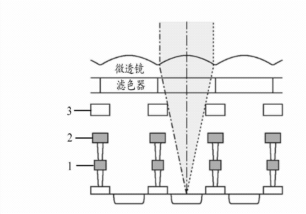
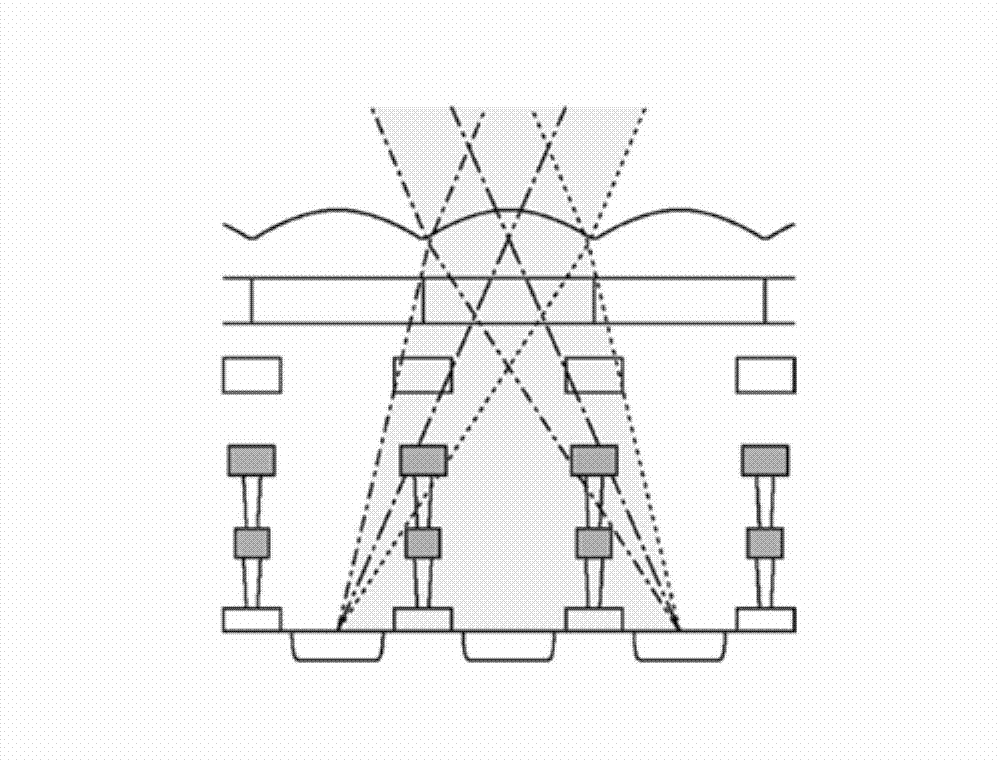
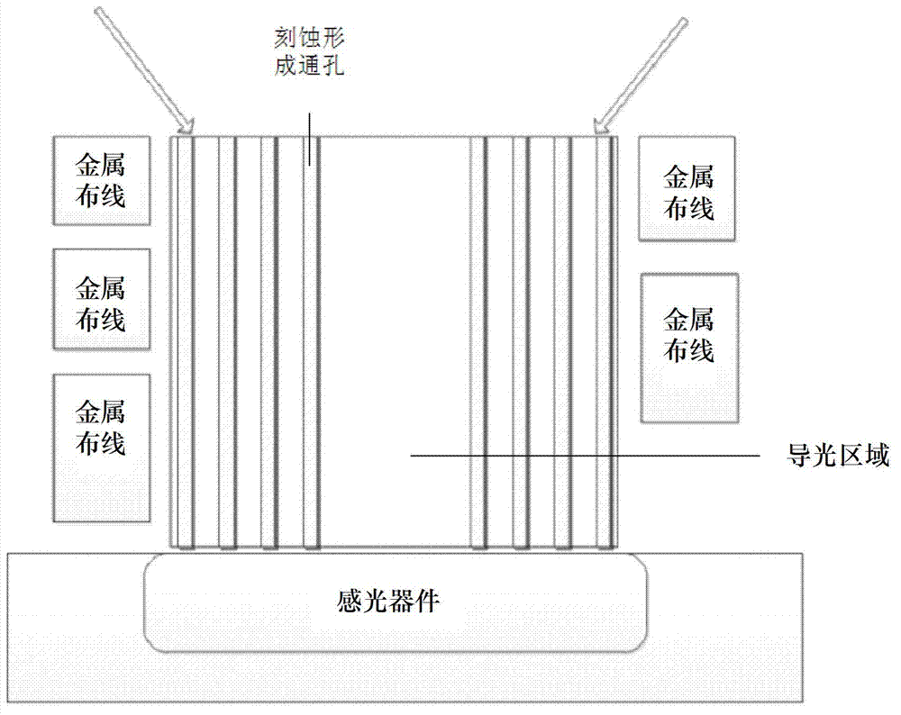
[0032] The first embodiment of the present invention relates to an image sensor. image 3 Is the schematic diagram of the image sensor, Figure 4 , Figure 5 , Image 6 These are top views of a dielectric layer in the image sensor, showing different arrangements of through holes.

[0033] Specifically, such as image 3 , Figure 4 As shown, the image sensor includ...


PUM


Abstract

The invention relates to the technical field of semiconductors, and discloses an image sensor and a preparation method thereof. In the image sensor, a plurality of columnar through holes are distributed in a dielectric layer above a photosensitive device of each photosensitive area to form a light guide area which is used for guiding light into a photosensitive device, and incident light can be bound in the light guide area to prevent light rays from being shot into adjacent pixel photosensitive areas during propagation to cause light crosstalk, so that the propagation route of the incident light in the light guide area is improved; and the transmission characteristics of the light guide area can be adjusted by controlling the parameters such as the pore size, the dielectric material, the distribution density and the like of the through holes in the light guide area, and controlling the arrangement mode of the through holes, so that an effect of improving the light intensity of the light shot into the light guide area is achieved. Moreover, based on the conventional image sensor circuit, a plurality of through holes are formed in the dielectric layer above the photosensitive area by using an etching and mat accumulation process, so that the image sensor is easy and convenient to operate and easy for mass production.

Description

technical field [0001] The invention relates to the technical field of semiconductors, in particular to an image sensor with a light guide area. Background technique [0002] As we all know, an image sensor is a semiconductor device that converts an optical image into an electrical signal. Image sensors can be roughly classified into two types: Charge-Coupled Device (CCD for short) and Complementary Metal Oxide Semiconductor (CMOS for short) image sensors. [0003] According to its readout method, the existing CMOS image sensors can be roughly divided into passive pixel sensor (Passive Pixel Sensor, referred to as "PPS"), active pixel sensor (Active Pixel Sensor, referred to as "APS") and digital pixel sensor There are three types of sensors (Digital Pixel Sensor, referred to as "DPS"). [0004] figure 1 with figure 2 are the photosensitive conditions in the image sensor structure under ideal conditions and actual conditions, respectively. [0005] Such as figure 1 As...

Claims


Application Information

Patent Timeline
IPC IPC(8): H01L27/146
Inventor 田犁方娜汪辉苗田乐陈杰
Owner SHANGHAI ADVANCED RES INST CHINESE ACADEMY OF SCI
Why Eureka
Try Eureka