
A photoelectric detection circuit

A photoelectric detection and photodetector technology, which is applied in the field of optical communication, can solve the problems that the leakage current of multi-channel selection switch affects the photoelectric detection results, etc., and achieve the effects of accurate detection, improved detection range and guaranteed accuracy

Active Publication Date: 2015-09-09
GUANGXUN SCI & TECH WUHAN
View PDF4 Cites 2 Cited by
  • Summary
  • Abstract
  • Description
  • Claims
  • Application Information

AI Technical Summary

Problems solved by technology

[0005] In view of the above problems, the object of the present invention is to provide a photoelectric detection circuit, which aims to solve the leakage of the multi-channel selection switch when the optical power of the optical signal to be measured is small due to the use of the existing photoelectric detection circuit. The current seriously affects the technical problems of photoelectric detection results

Method used


Image

  • A photoelectric detection circuit
  • A photoelectric detection circuit
  • A photoelectric detection circuit

Examples


Embodiment 1

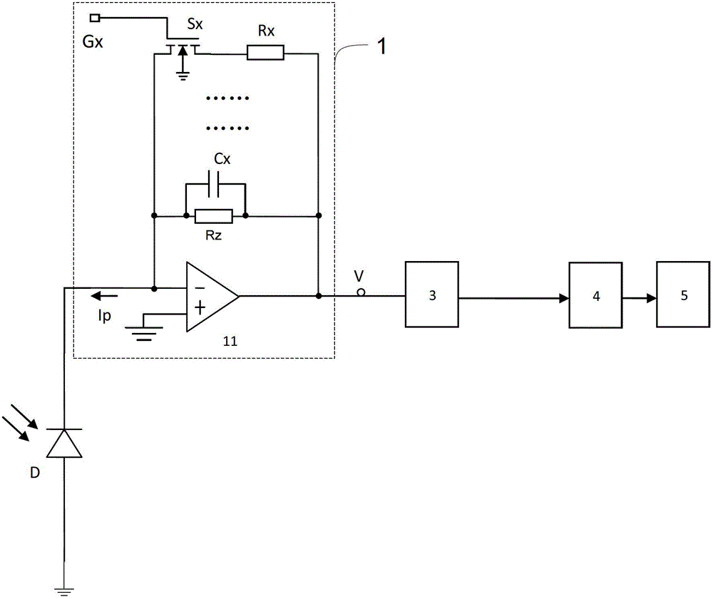
[0017] figure 2 The circuit structure of the photodetection circuit provided by the first embodiment of the present invention is shown, and only the parts related to the embodiment of the present invention are shown for convenience of description.

[0018] The photoelectric detection circuit provided in this embodiment includes a gain amplifier circuit 1, the input end of the gain amplifier circuit 1 is connected with a photodetector D, and the output end is connected with a control unit 4 and a display unit 5 in sequence, and the gain amplifier circuit 1 includes an operational amplifier 11, the inverting input terminal of the operational amplifier 11 is connected to the photodetector D, the non-inverting input terminal is grounded, the output terminal of the operational amplifier 11 is connected to the control unit 4, and the inverting input terminal of the operational amplifier 11 is connected to the control unit 4. A feedback resistor Rz is also connected between the phas...

Embodiment 2

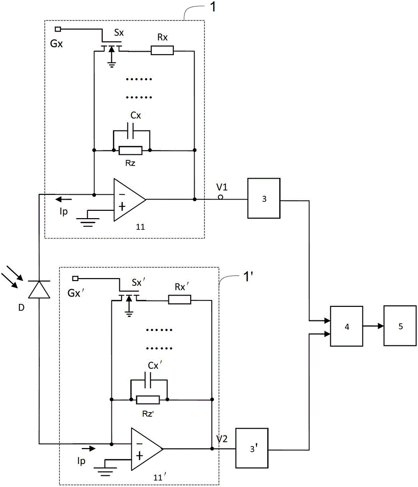
[0024] image 3 The circuit structure of the photodetection circuit provided by the second embodiment of the present invention is shown, and only the parts related to the embodiment of the present invention are shown for convenience of description.

[0025]The photodetection circuit provided in this embodiment includes two gain amplifier circuits 1, 1' as described in Embodiment 1, and the photodetector D is connected to the inverting input terminal of the operational amplifier in the two gain amplifier circuits. Between, the output terminals of the operational amplifiers 11, 11' are connected to the control unit 4, and their output voltages are V1 and V2 respectively, and the control terminals of the CMOS switches Sx, Sx' in the two gain amplifier circuits Both are connected to the control unit 4, and the control unit 4 automatically adjusts the working state (on or off) of the CMOS switches Sx and Sx' according to the input voltage values ​​V1 and V2, and selects one of the ...

Embodiment 3

[0030] Figure 4 The circuit structure of the photodetection circuit provided by the third embodiment of the present invention is shown, and only the parts related to the embodiment of the present invention are shown for convenience of description.

[0031] This embodiment describes the technical solution of the present invention as a specific example. In this embodiment, the adjustment resistor Rx is R1-R4, and the feedback resistor is R 2N-1 , R 2N , the CMOS switch Sx is S1-S4, the control terminal is G1-G4, and the specific positions of each device are as follows Figure 4 shown.

[0032] In this embodiment, the gain amplifier circuit 1 has three gears: R1 gear (S1 is on, S3 is off), R3 gear (S1 is off, S3 is on) and R 2N-1 gear (S1 and S3 are both disconnected), these three gears correspond to output gains of G1=0dB, G3=40dB and G 2N-1 =80dB; gain amplifier circuit 1' also has three gears: R2 gear (S2 on, S4 off), R4 gear (S2 off, S4 on) and R 2N gear (S2 and S4 are...


PUM


Abstract

The invention is applicable to the field of optical communication and provides a photoelectric detection circuit. The photoelectric detection circuit comprises a gain amplification circuit, a photoelectric detector, a control unit and a display unit, the gain amplification circuit comprises an operational amplifier, an inverted input end of the operational amplifier is connected with the photoelectric detector, a normal phase input end is grounded, an output end of the operational amplifier is connected to the control unit, a feedback resistor and at least one group of adjusting access circuit are connected between the inverted input end and output end of the operational amplifier, each group of adjusting access circuit comprises an adjusting resistor and a complementary metal oxide semiconductor (CMOS) switch which are in a series connection, a control end of the CMOS switch is connected to the control unit, the working state of the CMOS switch is controlled by the control unit, and the resistance value of the feedback resistor is larger than that of the adjusting resistor. Compared with existing circuits, the photoelectric detection circuit has the advantages that the detection range of optical power is increased, and even a weak optical signal can be accurately detected.

Description

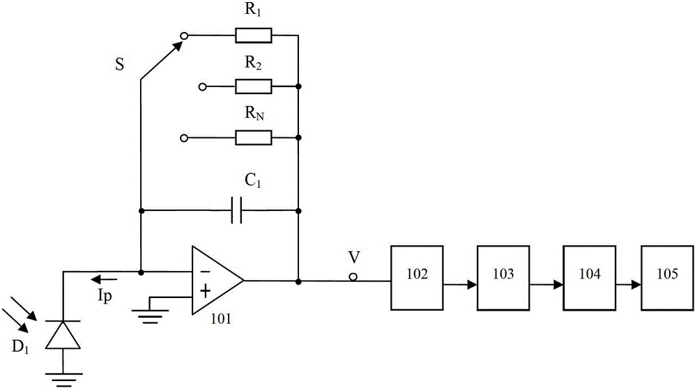
technical field [0001] The invention belongs to the field of optical communication, in particular to a photoelectric detection circuit. Background technique [0002] Photoelectric detection technology is a technology that converts light intensity information into processable electrical signals. It is a bridge between optical signals and electrical signals because of its long-distance, non-contact, fast and high-sensitivity detection and transmission. Its characteristics, as well as the advantages of high detection signal-to-noise ratio, strong anti-interference ability, and large information capacity, are widely used in the field of modern high-speed development of optical fiber communication. [0003] Such as figure 1 As shown, the existing multi-gain photoelectric detection circuit is composed of a photodiode D1, an operational amplifier 101, a multiplexer S, a feedback resistor R1 / R2 / RN, a feedback capacitor C1, a low-pass filter 102, and an analog-to-digital converter 1...

Claims


Application Information

Patent Timeline
Patent Type & Authority Patents(China)
IPC IPC(8): H04B10/07
Inventor 戈文杰喻杰奎胡强高罗清夏晓文张颖唐明星
Owner GUANGXUN SCI & TECH WUHAN
Learn More