A vacuum adsorption connection and binding process of IC card electronic chip and flexible circuit board

A flexible circuit board and electronic chip technology, which is applied in the direction of assembling printed circuits with electrical components, can solve the problems of high energy consumption of IC card electronic chips and radio frequency antennas, difficulty in achieving relevant technical parameters, and inability to re-use wafers, etc. To achieve the effect of guaranteed product quality, low production cost and high conductivity stability

Inactive Publication Date: 2015-11-25
湖南雅驰电子科技有限公司
View PDF6 Cites 0 Cited by
  • Summary
  • Abstract
  • Description
  • Claims
  • Application Information

AI Technical Summary

Problems solved by technology

[0002] At present, the country is vigorously promoting the development of the Internet of Things industry. IC cards, as radio frequency technology, are the basic hardware of the Internet of Things and are widely used in mobile phone cards, bus cards, bank cards, electronic access control, and electronic tags. In the assembly process of components, the traditional process is: first carry out "wafer packaging" (COB for short) on the IC card chip (that is, the silicon wafer of the IC card integrated circuit, also known as wafer), and then package the IC card electronically. The chip and the IC card induction coil (that is, the radio frequency antenna) are connected by welding, and then the IC card electronic components are packaged as a whole with PVC and other matrix materials, and it becomes various types of IC cards that we usually see. The assembly process of the components is firstly: lead (connect) the conductive solder pins and package the wafers, and the process requirements for guiding the solder pins from the wafers and packaging them are extremely high. Once a defective product occurs, it cannot be disassembled and repackaged. The element cannot be used twice, resulting in waste; at the same time, when the packaged IC card electronic chip and the radio frequency antenna are welded, the energy consumption is high, the pollution is large, and the relevant technical parameters are difficult to achieve accurate unity; moreover, the welding point is exposed in the air, which is easy The chemical reaction between the solder joint and the oxygen in the air, that is, the oxidation reaction, causes the connection failure of the solder joint

Method used


Image

  • A vacuum adsorption connection and binding process of IC card electronic chip and flexible circuit board

Examples


Embodiment Construction

[0018] The present invention will be further described below in conjunction with the accompanying drawings.

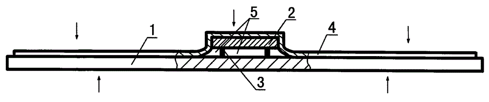
[0019] attached figure 1 Shown is a schematic diagram of the product structure processed by this process.

[0020] as attached figure 1 As shown, a vacuum adsorption connection binding process between an IC card electronic chip and a flexible circuit board is characterized in that the process it adopts is as follows:

[0021] In the first step, the processed and formed flexible circuit board 1 for producing IC cards is placed in a dust-free environment at normal temperature and pressure. In this environment, the contacts on the IC card electronic chip 2 are connected to the flexible circuit board The connection contacts 3 are connected correspondingly to each other, so that the printed circuit (i.e. radio frequency antenna or induction circuit) on the flexible circuit board is conducted with the internal circuit of the IC card electronic chip, in order to make the co...


PUM


Abstract

The invention discloses a vacuum adsorption connecting and binding process for an integrated circuit (IC) card electronic chip and a flexible printed circuit board. The process comprises the following steps of: butting connecting contacts of the IC card electronic chip and the flexible printed circuit board in a normal-temperature normal-pressure dustless environment; covering a plastic film layer on the connecting contacts; changing the original environment into a vacuum dustless environment, and pressing the plastic film on the flexible printed circuit board, so that a vacuum dustless small space is formed on an IC card electronic chip part between the plastic film and the flexible printed circuit board; and finally, taking the whole body formed in the process from the vacuum environment. The process is simple in operation process, low in manufacturing cost, reliable in product quality, energy-saving, environment-friendly and long in service life, and waste products are reduced.

Description

technical field [0001] The invention relates to an IC card, in particular to a technology for connecting and binding the electronic chip of the IC card and the flexible circuit board of the IC card by vacuum adsorption. Background technique [0002] At present, the country is vigorously promoting the development of the Internet of Things industry. IC cards, as radio frequency technology, are the basic hardware of the Internet of Things and are widely used in mobile phone cards, bus cards, bank cards, electronic access control, and electronic tags. In the assembly process of components, the traditional process is: first carry out "wafer packaging" (COB for short) on the IC card chip (that is, the silicon wafer of the IC card integrated circuit, also known as wafer), and then package the IC card electronically. The chip and the IC card induction coil (that is, the radio frequency antenna) are connected by welding, and then the IC card electronic components are packaged as a wh...

Claims


Application Information

Patent Timeline
Patent Type & Authority Patents(China)
IPC IPC(8): H05K3/32
Inventor 谢忠
Owner 湖南雅驰电子科技有限公司
Why Eureka
Try Eureka