An electro-static discharge protection circuit for an integrated circuit and a manufacturing method thereof

An electrostatic discharge and circuit protection technology, which is applied in the direction of circuits, electrical components, and electric solid devices, can solve problems such as premature aging of devices, reduced service life of integrated circuits, and damage, so as to prolong service life, improve utilization rate, reduce small size effect

Inactive Publication Date: 2013-03-20
SEMICON MFG INT (SHANGHAI) CORP
View PDF7 Cites 4 Cited by
  • Summary
  • Abstract
  • Description
  • Claims
  • Application Information

AI Technical Summary

Problems solved by technology

In an ideal state, when a certain moment is reached, the entire multi-finger GGNMOS circuit can be turned on, but the ESD current conducted by the middle part is still larger than the ESD current conducted by other parts, thus causing more heat. large, which can easily cause damage to the
However, in practical applications, the above-mentioned multi-finger GGNMOS circuit often only has an effect on the conduction of ESD current in the middle part, while the conduction effect of the edge part on the ESD current is negligible.
At the same time, due to the large conduction current in the middle part, the heat generated by it should not be dissipated quickly, which will easily cause premature aging of the device and reduce the service life of the integrated circuit.

Method used


Image

  • An electro-static discharge protection circuit for an integrated circuit and a manufacturing method thereof
  • An electro-static discharge protection circuit for an integrated circuit and a manufacturing method thereof
  • An electro-static discharge protection circuit for an integrated circuit and a manufacturing method thereof

Examples


Embodiment Construction

[0029] In order to make the object, technical solution and advantages of the present invention clearer, the present invention will be further described in detail below with reference to the accompanying drawings and examples.

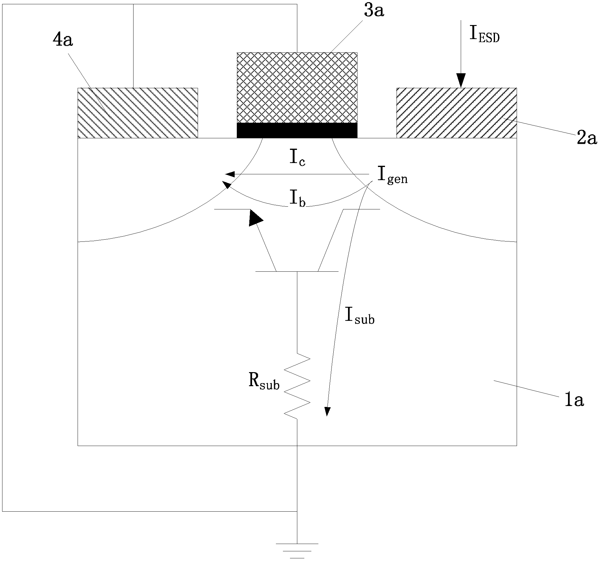
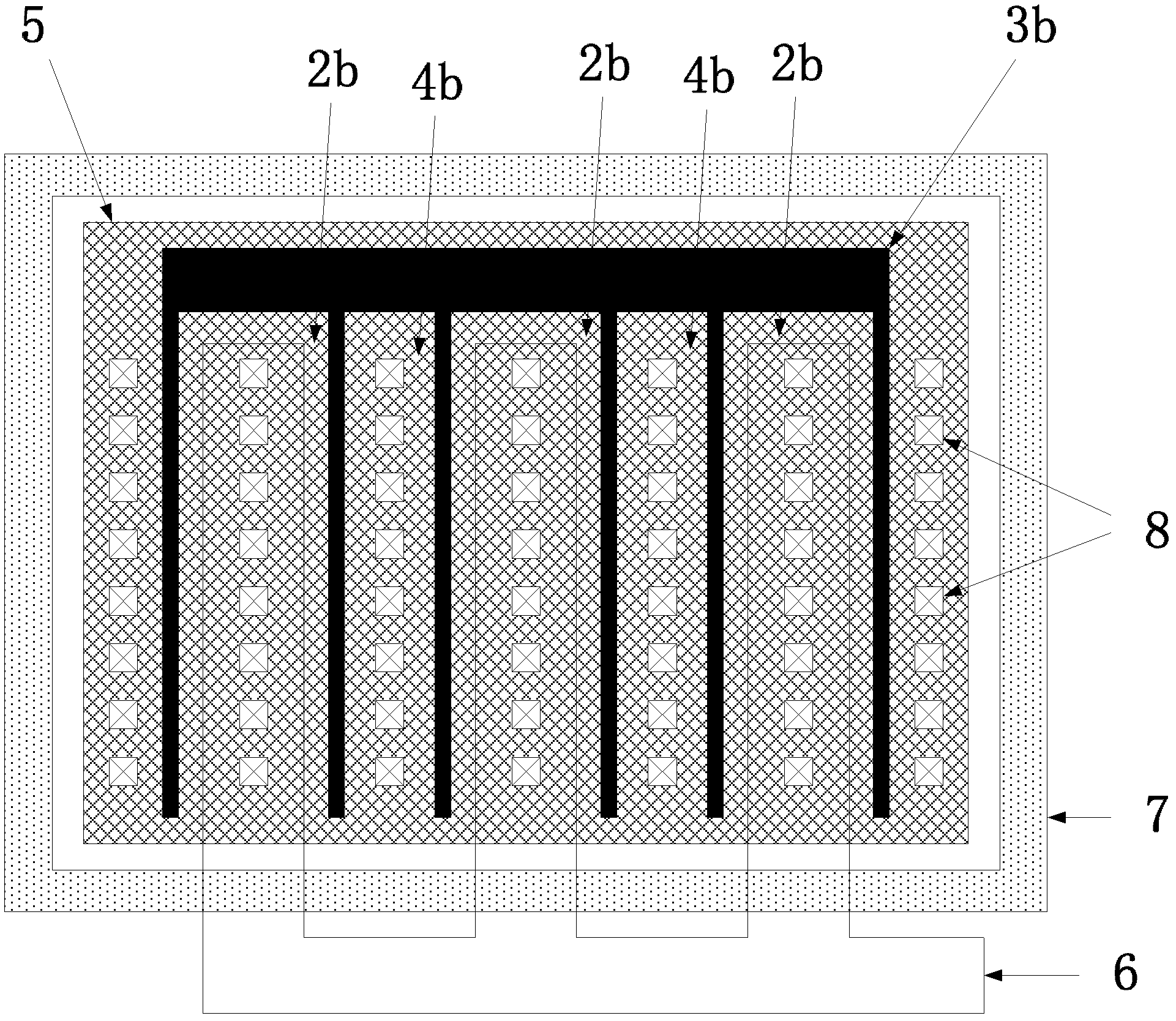
[0030] As a specific embodiment, the integrated circuit electrostatic discharge protection circuit structure of the present invention is as follows Figure 5shown. Without changing the size of the pick-up region 7 in the prior art, the length and width dimensions of the GGNMOS are reduced, that is, the length and width dimensions of the source and drain regions 5 are reduced, and the substrate between the source and drain regions 5 and the pick-up region 7 A plurality of through-silicon vias 9 (TSV, Through Silicon Via) are formed in it. Specifically, the structure of the integrated circuit electrostatic discharge protection circuit of the present invention is as follows: a source and drain region 5 is formed on the substrate, and the size of the sourc...


PUM


Abstract

The present invention discloses an electro-static discharge protection circuit for an integrated circuit and a manufacturing method thereof. The protection circuit includes a GGMOS and at least one through-silicon via which share the same substrate; and the silicon via is arranged in the substrate around the GGMOS. In the electro-static discharge protection circuit for the integrated circuit of the present invention, when the ESD (electro-static discharge) is produced, heat will be generated on the GGMOS due to the presence of the ESD current; by using the silicon via disposed in the substrate around the GGMOS, better and faster heat dissipation for the GGMOS can be achieved, thus preventing damage to the GGMOS caused by heat, and extending the service life of the electro-static discharge protection circuit; and GGMOS turn-on voltage adjustment can also be achieved by arrangement mode of silicon vias at the same time. According to the protection circuit, the size of the GGMOS is reduced, so that the entire region GGMOS is enabled to be completely open when the ESD is produced, thereby improving utilization rate of the GGMOS.

Description

technical field [0001] The invention relates to semiconductor manufacturing technology, in particular to an integrated circuit electrostatic discharge protection circuit and a manufacturing method thereof. Background technique [0002] ESD (Electro-Static discharge, electrostatic discharge) is a rapid neutralization process of charges. Due to the high electrostatic voltage, ESD will bring destructive consequences to the integrated circuit, resulting in the failure of the integrated circuit. Therefore, in order to protect the integrated circuit from being damaged by ESD, an ESD protection circuit is also designed in the integrated circuit to prevent the integrated circuit from being damaged by ESD. [0003] In CMOS (Complementary Metal Oxide Semiconductor, Complementary Metal Oxide Semiconductor) technology, NMOS (N-Metal-Oxide-Semiconductor, N-type Metal Oxide Semiconductor) devices include parasitic lateral npn transistors. At present, GGNMOS (Gate Grounded NMOS, gate gro...

Claims


Application Information

Patent Timeline
Patent Type & Authority Applications(China)
IPC IPC(8): H01L27/02H01L23/367
Inventor 甘正浩张莉菲
Owner SEMICON MFG INT (SHANGHAI) CORP
Why Eureka
Try Eureka