Write-through lithography processing system and lithography method

A lithography processing and direct writing technology, applied in the field of lithography, can solve the problems of low processing efficiency and high cost of precision optical scanning device equipment, and achieve the effect of low coherence requirements and good flexibility

Inactive Publication Date: 2013-03-27
SUZHOU UNIV
View PDF5 Cites 23 Cited by
  • Summary
  • Abstract
  • Description
  • Claims
  • Application Information

AI Technical Summary

Problems solved by technology

But its main problem is the single-point scanning processing method, the processing efficiency is very low, and the equipment cost of the precision optical scanning device used is very high
[0017] In short, the existing processing methods cannot directly, efficiently, precisely and cost-effectively produce large-scale precision curved surface microstructures

Method used


Image

  • Write-through lithography processing system and lithography method
  • Write-through lithography processing system and lithography method
  • Write-through lithography processing system and lithography method

Examples


Embodiment Construction

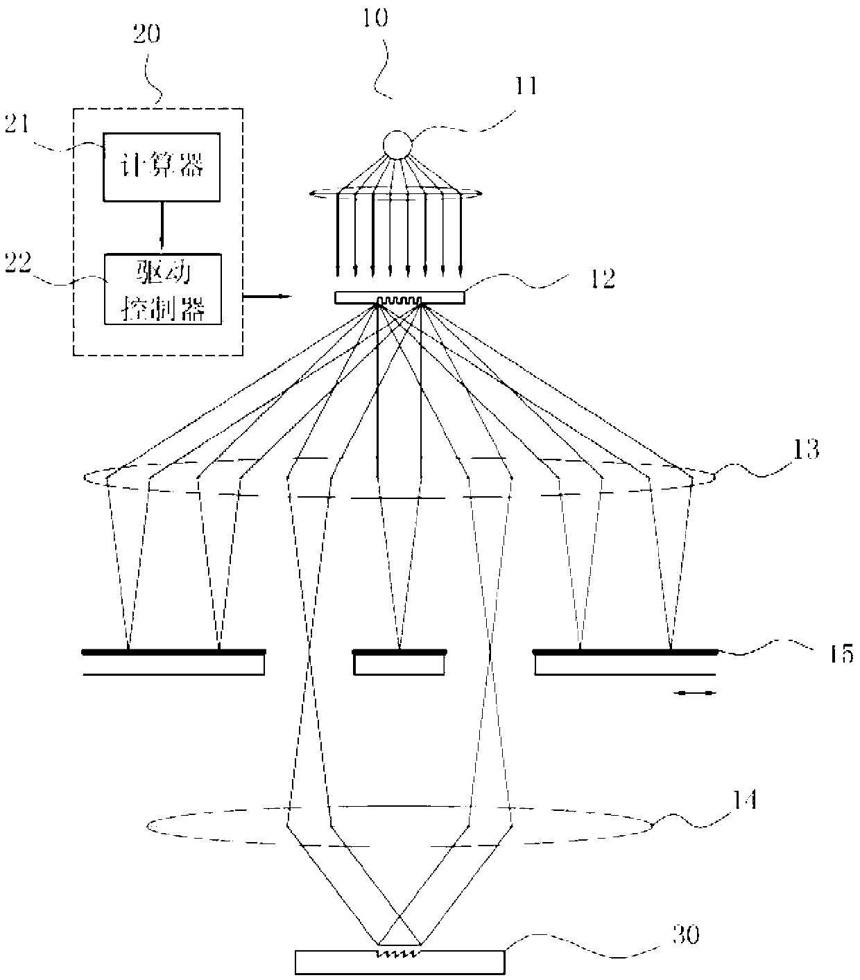
[0050] See figure 2 , figure 2 It is a structural schematic diagram of the direct writing photolithography processing system of the present invention. As shown, the system includes an exposure system 10 and a control system 20 . The exposure system 10 is essentially an exposure optical path for producing two-beam interference exposure, including a light source 11 , a spectroscopic device 12 , a first optical mirror group 13 , an iris diaphragm 15 and a second optical mirror group 14 . The exposure system 10 composes the exposure optical path in the order of a light source 11 , a spectroscopic device 12 , a first optical mirror group 13 , an iris diaphragm 15 and a second optical mirror group 14 .

[0051] In a preferred embodiment, the light source 11 adopts a laser, which has the advantage that the laser has good coherence and is suitable for interference lithography. In addition, compared with ordinary light sources, laser has good uniformity of light field. The use of...


PUM

PropertyMeasurementUnit
sizeaaaaaaaaaa

Abstract

The invention provides a write-through lithography processing system and a lithography method. The photolithography processing system comprises a control system capable of using Fourier for calculating and an exposing system controlled by the control system to achieve repeated lithography. The lithography method enables a curved surface to be etched to be unfolded into Fourier polynomial according to a Fourier analysis principle, performs repeated lithography according to cosine functions in the polynomial, and achieves etching of a target curved surface after overlaying of repeated lithography. The write-through lithography processing system and the lithography method can etch any large-format three-dimensional curved surface and have the advantages of being high in design flexibility, etching efficiency and accuracy, low in cost and the like.

Description

technical field [0001] The invention belongs to the technical field of photolithography, and in particular relates to a direct-writing photolithography processing system and a photolithography method for preparing three-dimensional curved surfaces. Background technique [0002] Three-dimensional curved surface (micro) structures are widely used in many fields such as optical films, flat panel displays, micro-optical devices, and micro-electromechanical systems (MEMS). For example, a microlens array with a spherical structure, also known as a fly-eye lens, can achieve beam homogenization and array imaging, and is widely used in photolithography machine light source and CCD detection and other fields. Another example is the optical film with V-shaped groove and pyramid structure, which has the optical effect of directional reflection, and is widely used in safety signs in the field of public transportation. [0003] At present, there are three main methods of fabricating thre...

Claims


Application Information

Patent Timeline
Patent Type & Authority Applications(China)
IPC IPC(8): G03F7/20
Inventor 胡进浦东林陈林森
Owner SUZHOU UNIV
Why Eureka
Try Eureka