
Method for optimizing CDSEM (Critical Dimension Electronic Microscope) running sequence

A sequential, out-of-stock technology, applied in the direction of semiconductor/solid-state device testing/measurement, can solve the problems of high cost, low utilization rate of CDSEM, and high cost of CDSEM system, so as to reduce waiting time, improve production efficiency, and increase utilization rate Effect

Active Publication Date: 2013-03-27
SHANGHAI HUALI MICROELECTRONICS CORP
View PDF4 Cites 14 Cited by
  • Summary
  • Abstract
  • Description
  • Claims
  • Application Information

AI Technical Summary

Problems solved by technology

[0005] The present invention aims at providing an optimized CDSEM system for the defects of the prior art that the cost of the traditional CDSEM system is expensive and the cost is too high, and the limited number of CDSEM purchased by the semiconductor company has a low utilization rate and cannot meet the needs of actual production and research and development. sequential method

Method used


Image

  • Method for optimizing CDSEM (Critical Dimension Electronic Microscope) running sequence
  • Method for optimizing CDSEM (Critical Dimension Electronic Microscope) running sequence

Examples


Embodiment Construction

[0019] In order to illustrate the technical content, structural features, achieved goals and effects of the present invention in detail, the following will be described in detail in conjunction with the embodiments and accompanying drawings.

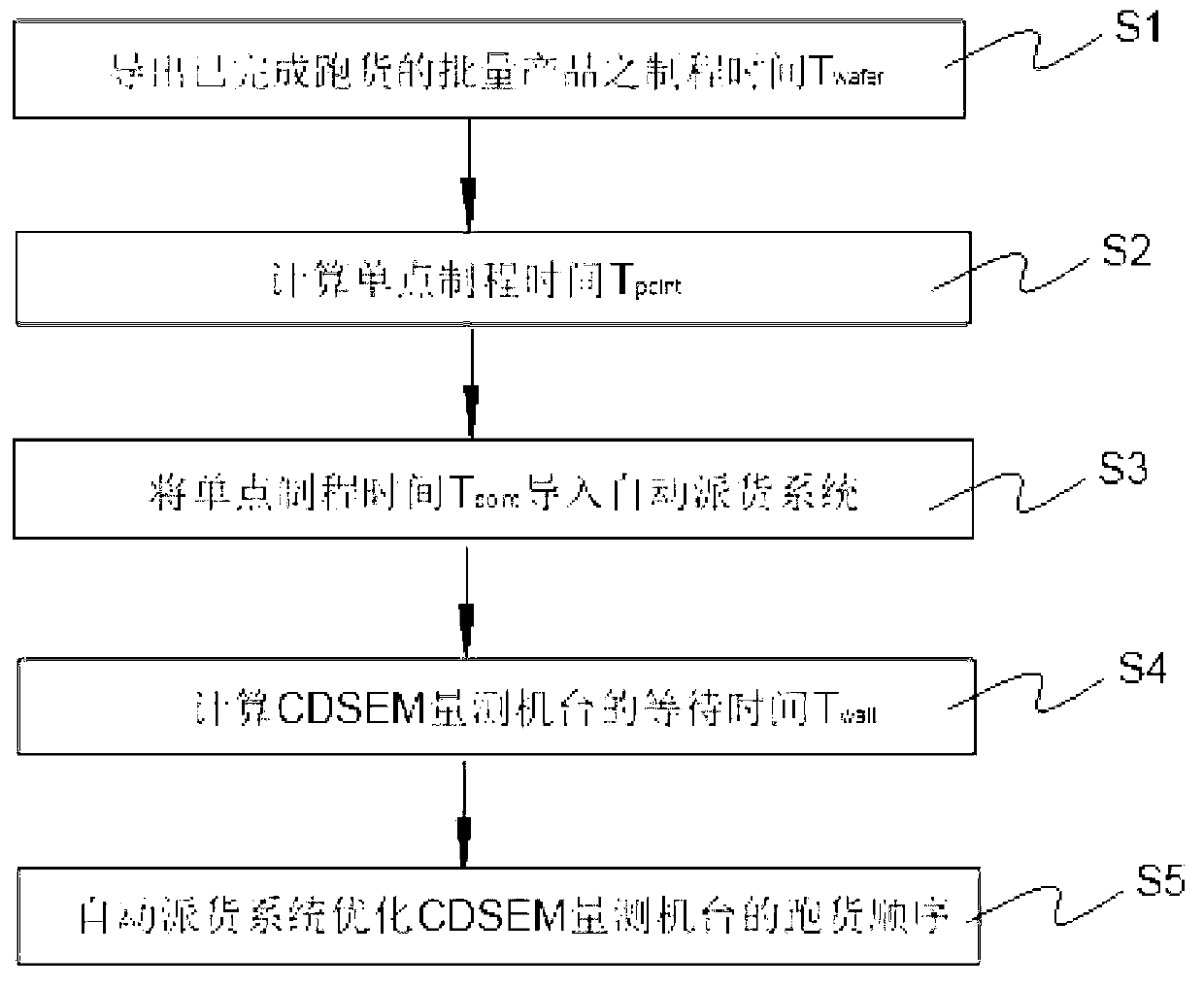
[0020] see figure 1 , figure 1 Shown is a flow chart of a method for optimizing CDSEM running order of the present invention. The method for described optimization CDSEM running order, comprises the following steps:

[0021] Execute Step S1: Use CDSEM to measure the prescription browser software to export the process time T of the batch products that have been shipped wafer ;

[0022] Execute step S2: Calculate the single-point process time T point ; Specifically, through the setting of the measurement program, combined with the CDSEM measurement prescription browser software, the process time T of the batch products that have completed the running goods is exported wafer , and according to the formula Calculate the single point p...


PUM


Abstract

The invention relates to a method for optimizing CDSEM (Critical Dimension Electronic Microscope) running sequence, comprising the following steps: step S1, exporting wafer time Twafer of high volume products after running; step S2, counting single-point wafer time Tpoint; step S3, importing the single-point wafer time Tpoint in an automatic dispatching system; step S4, counting waiting time Twait of a CDSEM measuring board; and step S5, optimizing the running sequence of the CDSEM measuring board according to the waiting time Twait obtained in the step S4 and the priority level sequence of high volume products recorded in the automatic dispatching system by the automatic dispatching system. The method for optimizing CDSEM running sequence realizes the quantification of the waiting time of the CDSEM measuring board, and optimizes the running sequence of the CDSEM measuring board combined with the related information of priority level sequence of the high volume products recorded by the automatic dispatching system, amount of measuring points, and the like, thereby not only improving the utilization rate of the CDSEM measuring board but also shortening the waiting time of the high-level high volume products at the CDSEM measuring board and greatly improving the production efficiency.

Description

technical field [0001] The invention relates to the technical field of semiconductor devices, in particular to a method for optimizing the order of CDSEM shipments. Background technique [0002] Currently, in the manufacture of semiconductor devices, a critical dimension scanning electron microscope (Critical Dimension Electronic Microscope, CDSEM) is used to measure the critical dimension (Critical Dimension, CD) of a pattern fabricated on a wafer. With the development of semiconductor technology, the critical dimensions of semiconductor devices are getting smaller and smaller. In order to ensure the accuracy of the pattern on the wafer after photolithography or etching, after the pattern on the mask is transferred to the wafer after exposure and development, the wafer with the pattern will be placed on the CDSEM machine, and the CDSEM machine will be controlled by the CDSEM control system Measure the critical dimensions of the pattern after lithography, and the CDSEM mach...

Claims


Application Information

Patent Timeline
IPC IPC(8): H01L21/66
Inventor 夏婷婷朱骏马兰涛张旭升
Owner SHANGHAI HUALI MICROELECTRONICS CORP
Features
  • Generate Ideas
  • Intellectual Property
  • Life Sciences
  • Materials
  • Tech Scout
  • Unparalleled Data Quality
  • Higher Quality Content
  • 60% Fewer Hallucinations
Learn More